A precise maze on a wafer is consuming billions in R&D funds and market opportunities.
In June 2025, the semiconductor industry faced a silent “avalanche.” According to the latest data from Siemens EDA: the global chip tape-out success rate has plummeted to a historic low of 14%, meaning that eight out of ten design companies have fallen into the tape-out “valley of death.” Two years ago, this figure was still 24%, and even earlier, the industry average was around 30%. Behind this technical winter lies a conundrum of soaring chip complexity, compressed development cycles, and the demand for AI computing power.

1. Tape-out Failures: A Chain Reaction from “Design Verification” to “Commercial Disaster”
Tape-out is referred to by engineers as the “moment that distinguishes heaven from hell”—when the chip samples return from the foundry, pressing the RESET button determines the fate of tens of millions in R&D investment.
-
Cost Black Hole: The cost of a single tape-out can reach millions to tens of millions of dollars depending on the process. Failure not only means evaporating funds but also leads to a product launch delay of 6-12 months.
-
Competitive Stagnation: AMD once lost market share to Intel’s Sandy Bridge after the tape-out of the Bulldozer architecture did not meet performance expectations; Qualcomm’s Snapdragon 810 ceded the high-end smartphone market to Samsung’s Exynos due to overheating issues post-tape-out.
-
Hidden Failures: Even if functionality is normal, if performance is below expectations by 10% (such as excessive power consumption or insufficient speed), the chip will lose market competitiveness and be forced to re-tape-out.
2. Four Major Technical Strangulations: Tightening the Lifeline of Tape-out
1. Exponential Increase in Complexity
Modern chips have shifted from “single-chip integration” to multi-chip heterogeneous integration (e.g., using 5nm for computing cores and 14nm for storage units). Server chips need to coordinate different process nodes and multiple foundries, leading to a geometric increase in design verification complexity.
2. The Double-Edged Sword of Custom Chips
There has been a surge in custom chips for scenarios like AI and automotive. For example, deep learning chips require restructured architectures and instruction sets for neural networks, resulting in a verification workload far exceeding that of general-purpose chips. By 2025, custom chips accounted for 67% of tape-out projects, doubling from three years ago.
3. Leap in Development Cycles
The industry development cycle has been compressed from 18 months to less than 12 months. Companies, in a bid to seize market windows, are forced to cut verification steps:
-
A certain GPU manufacturer reduced verification coverage from 99% to 92%
-
Key path simulation time was shortened by 40%
leading to a 30% increase in potential defect miss rates.
4. AI Computing Power Demand Forces Design Limits
“The demand for computing power from AI is surging, far exceeding the pace of semiconductor technology advancement. Engineers can only use outdated tools to complete more work in a shorter time,” noted semiconductor engineering editor Brian Bailey. The computing power requirements for large model chips double every three months, while the efficiency growth of EDA tools is less than 15% per year.
3. Path to Breakthrough: From “Going Solo” to Ecological Collaboration
Faced with a cliff of 14% success rate, the industry is exploring three survival paths:
1. AI Restructuring Chip Design Processes
-
Intelligent Verification: Google uses reinforcement learning algorithms to improve bug detection rates by 40%
-
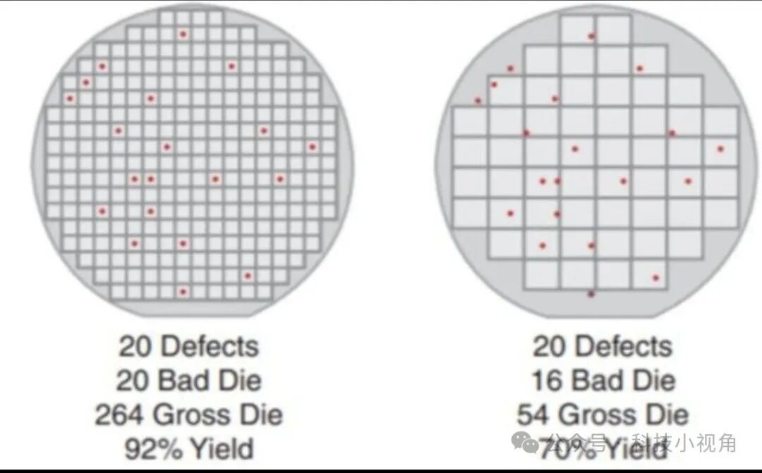
Predictive Modeling: TSMC’s key to achieving over 60% yield at 2nm is embedding AI into the process defect prediction system
2. Specialized Division of Labor Creates ASIC Service Giants
Design companies are outsourcing modules to specialized IP suppliers. ARM’s Neoverse V3 core licensing has increased by 200% annually, and the Chiplet ecosystem diversifies tape-out risks.
3. Quality Joint Defense Across the Entire Industry Chain
The secret to TSMC achieving 80% yield at 3nm is establishing over 2000 monitoring nodes from wafer procurement to photoresist coating. Intel’s 18A process has reduced defect response time to 4 hours through real-time feedback systems using EUV equipment.
Future Outlook: Technological Evolution Amidst the Winter
As Moore’s Law approaches physical limits, the plummeting tape-out success rate is indeed a growing pain of technological evolution. Just as the success rate dropped by 26% during the transition from 28nm to 14nm in 2018, the current low point during the transition to 2nm/GAA processes will eventually be overcome.
As Intel Vice President John Pitzer stated: “The confidence of the 18A process in comparison to TSMC’s N2 comes from innovations across the entire chain of technology.” In this “survival game” of chip design, the ultimate winners will be those who embed AI genes into the design bloodstream and replace closed development with open ecosystems.
Data Source: Siemens EDA Report/Semiconductor Engineering Analysis (2025)
Like Share Happiness Forever🌷Light Up Heart❤ Happy Every Day!

Seeking Likes
Seeking Shares
Seeking Views
Seeking Comments