One of the key requirements for developing modern integrated quantum sensor devices is to seamlessly integrate the sensors into existing tool systems. In the field of high-pressure science, the recently introduced nitrogen-vacancy (NV) centers in diamond anvil cells (DAC) provide a powerful demonstration, enabling in-situ characterization of stress and magnetism under extreme pressures, thus promoting advancements in various fields such as materials science and geology.
However, this implementation still has limitations: the NV layer implanted beneath the culet of the diamond anvil is located outside the sample chamber, thus restricting proximity to the target sample. In contrast, nanodiamonds placed inside the chamber can get closer to the sample, but the randomness of the position and crystal orientation of the nanodiamond particles in this geometric structure makes it difficult to perform wide-field imaging tasks.
To address these issues, they proposed using negatively charged boron-vacancy (VB−) centers embedded in layered hexagonal boron nitride (hBN) as an alternative high-pressure sensing platform within the DAC. The VB− centers and other recently discovered van der Waals material spin defects provide a new approach for constructing quantum sensor devices.
In principle, the atomic-scale thin structure of the host material allows the two-dimensional sensor to be placed at sub-nanometer distances from the target sample, enabling unprecedented sensitivity and resolution for imaging interface phenomena. Furthermore, the two-dimensional sensors can be easily integrated with other two-dimensional devices through three-dimensional heterogeneous integration, thus promoting large-scale manufacturing of the next generation of microelectronic devices.
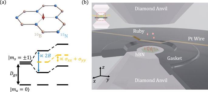
In this study, the team led by Assistant Professor Chong Zu from the University of Washington’s Department of Physics primarily demonstrated three achievements. First, they directly transferred a film of hBN approximately 100 nm thick, containing VB− centers, to the surface of the diamond anvil’s culet (Figure 1). They systematically studied the electronic spin properties of the VB− centers under pressures of up to 3.5 GPa. The pressure-induced spin level shift of the VB− centers was measured to be (2π)×(43 ± 7) MHz/GPa, which is consistent with first-principles calculations but significantly different from previous results obtained from direct weight application on hBN.
Notably, the pressure response of the VB− centers is about three times that of the NV centers in diamond, highlighting their potential as in-situ pressure and stress sensors. Secondly, they used the VB− sensors to directly map the stress distribution and gradient inside the high-pressure chamber. When using sodium chloride (NaCl) as the pressure medium, they found that the stress environment began to become uneven at around 2 GPa, which is consistent with existing studies.
Finally, they demonstrated the ability of the VB− centers to image magnetic fields in heterogeneous devices by studying the pressure-tuned magnetism in the room-temperature intercalated van der Waals ferromagnet Cr₁₊δTe₂, observing a transition from ferromagnetic to non-magnetic states at around 0.5 GPa, which can be explained by the weakening of exchange interactions.