This is a professional guide for PCB layout and wiring for the SPI interface, focusing on core challenges such as high-speed clock synchronization, signal group timing matching, and anti-crosstalk:

1. SPI Interface Characteristics and Design Challenges
|
Characteristics |
Design Impact |
|
Full-Duplex Communication |
MOSI/MISO must be routed independently to avoid coupling interference |
|
Synchronous Clock |
The SCK signal must be strictly equal in length (deviation ≤ 50 mil), clock jitter directly affects the sampling window |
|
Multi-Slave Topology |
The length of the chip select signal (CS) traces must match to prevent selection delays that lead to timing errors |
|
High Speed |
For speeds >50MHz, transmission line treatment is required (impedance control, termination matching) |

2. Key Layout Rules
1. Device Topology Optimization
Place master and slave devices close together
Recommended: Master ── Slave1 (Distance ≤ 5cm) └─ Slave2 (Distance ≤ 5cm) // Daisy chain topologyAvoid: Master ─┬─ Slave1 (Distance 10cm) └─ Slave2 (Distance 3cm) // Unequal branch lengths cause timing offsets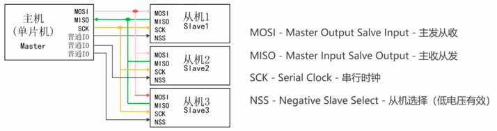
Independent layout for chip select signals (CS)
Each CS signal must be routed separately, shared traces are prohibited
CS signal source end should be in series with a 22Ω resistor (to suppress reflections)
2. Key Signal Grouping
|
Signal Group |
Included Signals |
Layout Requirements |
|
Clock Group |
SCK |
Shortest path, away from high-speed noise sources |
|
Data Group 1 |
MOSI + related GND |
Spacing ≥ 3 times the line width from MISO group |
|
Data Group 2 |
MISO + related GND |
Offset layout when routed parallel to MOSI group |
|
Control Group |
CS1, CS2… |
Equal length matching (within group deviation ≤ 100 mil) |

🛠️ 3. High-Speed Wiring Specifications
1. Key Parameters for Signal Lines
|
Signal |
Line Width |
Spacing Requirements |
Length Matching |
|
SCK |
0.15-0.2mm |
≥ 2 times line width from other signals |
Reference Signal |
|
MOSI |
0.15-0.2mm |
≥ 3 times line width from MISO |
Deviation from SCK ≤ ±50 mil |
|
MISO |
0.15-0.2mm |
≥ 3 times line width from MOSI |
Deviation from SCK ≤ ±50 mil |
|
CSx |
0.12-0.15mm |
≥ 2 times line width from each other |
Within group deviation ≤ ±100 mil |
2. Timing Control Techniques
Equal Length Serpentine Lines:
SCK total length = reference length MOSI length = SCK length ±50 mil // Serpentine amplitude ≤ 4 times line width, spacing ≥ 2 times line widthTermination Matching (required for >50MHz):
Series Resistor at Source End: SCK/MOSI should be in series with a 22-33Ω resistor close to the master control end (within 300 mil from the pin)
Parallel Resistor at Far End: MISO should be in parallel with 50Ω to GND at the slave end (only used when the topology is star-shaped)
3. Shielding and Isolation
Ground Plane Treatment:
GND ──┬───────┬─────── GND │ SCK │ GND ──┼───────┼─────── GND // Ground width ≥ 2 times signal line width │ MOSI │ GND ──┼───────┼─────── GND │ MISO │ GND ──┴───────┴─────── GND Place a via every 200 mil on the ground line (via diameter ≥ 0.3mm)
Cross-Division Treatment: When signal lines change layers, place a return ground via next to the via (spacing ≤ 100 mil)

4. Power and Ground Design
Power Filtering
Add a 0.1μF ceramic capacitor to the VCC pins of the master and slave devices (positioned close to the pins, loop ≤ 2mm)
For high-speed SPI (>50MHz), additionally add a 1μF ceramic capacitor + ferrite bead filter (e.g., 600Ω@100MHz)
Ground Plane Strategy
Complete Ground Plane: A continuous ground plane must be maintained under SPI signals (no segmentation allowed!)
Single Point Grounding: For analog devices (e.g., ADC connected via SPI), use star grounding, with the grounding point selected at the master control GND pin

5. Noise Suppression and EMC
Crosstalk Suppression
MOSI and MISO should use vertical crossing traces or increase spacing to 5 times line width
Adjacent signal layer routing directions should be orthogonal (e.g., L1 layer horizontal, L2 layer vertical)
Clock Jitter Optimization
Place GND Guard Trace on both sides of the SCK signal (ground protection line), width ≥ 2 times the signal line
Avoid placing the SCK line close to the board edge (distance ≥ 3mm)
ESD Protection
If the SPI connector is exposed, add a bidirectional TVS diode at the interface (Vrwm=3.3V/5V, Vc<8V)
Connect the TVS diode ground pin directly to the metal shell (not signal ground)

⚙️ 6. High-Speed Scenario Enhancement Solutions
1. Designs over 50MHz
Impedance Control:
Surface microstrip: 50Ω (when FR4 board thickness is 1.6mm, line width ≈ 0.3mm)
Inner stripline: 50Ω (line width ≈ 0.2mm, PP sheet thickness 0.2mm)
Shorten Traces: Total bus length < 110×cf101×fc (e.g., for 100MHz, length < 15cm)
2. Multi-Slave Systems
Use Buffers: e.g., SN74LVC4245, to split total bus load
Hierarchical Clocking:
Master → Clock Buffer → SCK1 → Slave1 → SCK2 → Slave2 // Each branch independently terminated

7. Debugging and Verification Points
Test Point Design
Reserve 4-channel test points: SCK, MOSI, MISO, CS (grouped, spacing 2.54mm)
Test point lead length ≤ 5mm to avoid introducing additional delays
Signal Quality Testing
Key Indicators:
SCK rise time < 0.2 × clock period
MOSI/MISO setup time > 5ns (relative to SCK edge)
Overshoot voltage < 15% Vdd

Core Design Mnemonics
Equal clock length is fundamental, data group spacing three timesGround via protects signals, termination resistors suppress reflectionsPower decoupling close to chips, ground plane continuous and uninterruptedHigh-speed routing controls impedance, multi-slave uses buffers
Following this guide ensures stable transmission of the SPI bus at 100MHz clock, passing EN 55032 Class B radiation certification. After wiring, it is recommended to use TDR to check impedance continuity and verify timing margins with eye diagrams (>40% UI is safe).