In a DC-DC power circuit, the layout of the PCB is crucial for the implementation of circuit functionality and achieving good performance metrics. Today, we will take the Buck circuit as an example to analyze how to perform a reasonable PCB layout and the considerations in the design.
↓ Click to watch the video explanation ↓
1. Power Circuit
As shown in Figures1(a) and 1(b), the current loops during the turn-on and turn-off of the upper switch are displayed, which we commonly refer to as the power circuit section. This part of the circuit is responsible for supplying power to the user load and handles a significant amount of power. The upper and lower switches in the circuit typically use MOS transistors, controlled by the PWM signals generated internally by the chip to perform high-speed switching. The inductors and capacitors in the latter part of the circuit form an LC filter circuit, thus avoiding a significant current change trend.
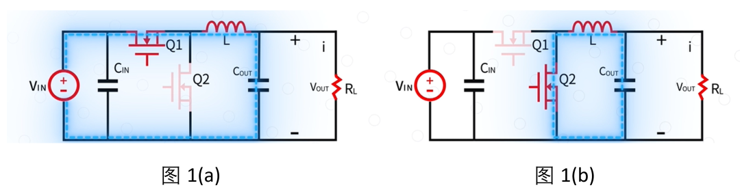
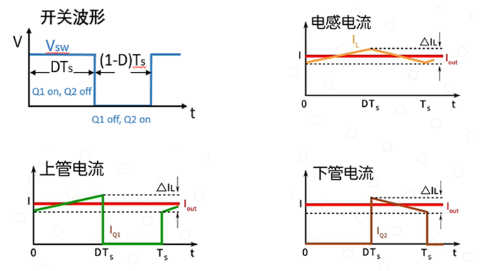
Figure1(c)
Combining the current waveforms of the upper and lower switches, namely Q1 and Q2 (Figure 1(c)), it is not difficult to find that a high current transition rate occurs only in the sections of the two switching transistors. Due to the rapid voltage changes of the PWM signal, the SW point generates strong noise. Therefore, when routing the PCB, special attention is needed to minimize the area of this rapid change loop to reduce interference with other parts. Fortunately, with advancements in integration technology, most power chips now integrate the upper and lower switches within the chip, with only a few applications requiring external MOS or diodes.
2. PCB Layout of the Power Circuit
For a typical Buck chip, its inductor charging power circuit includes input capacitors, the integrated upper switchMOSFET, power inductors, and output capacitors and other components. The inductor discharging power circuit includes power inductors, output capacitors, and the integrated lower switchMOSFET, etc.
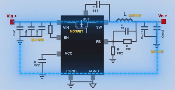
Figure2(a) Inductor charging power circuit
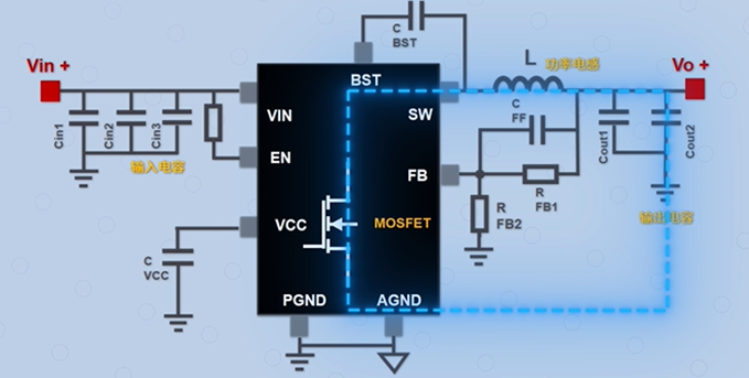
Figure2(b) Inductor discharging power circuit
When performing PCB routing, these two power circuits should be as short and thick as possible, maintaining a small loop area while ensuring current-carrying capacity, which can reduce noise radiation.
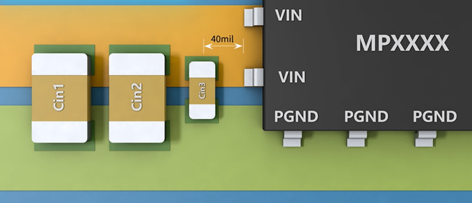
Input Capacitor: should be placed close to the chip’s input Vin and power ground PGND to reduce parasitic inductance. Because the input current is discontinuous, noise caused by parasitic inductance may exceed the chip’s voltage tolerance and adversely affect the logic units.VIN pins should have at least 1 decoupling capacitor nearby, ideally less than 40mil, to filter out AC noise from the power input and noise from the chip (backfeeding), while also serving as energy storage.
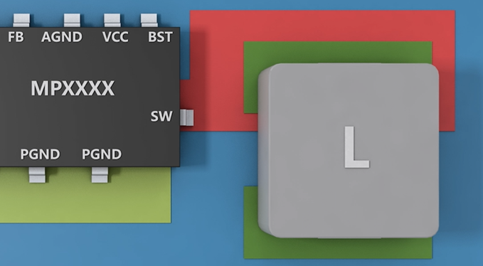
SW Point: is the switching node and a noise source, so it should maintain as small an area as possible while ensuring current flow, and be kept away from signal lines that are susceptible to interference. Additionally, it is important to note that for high current applications of Buck circuits, avoid placing vias at the SW point to prevent noise from being transferred to other layers.
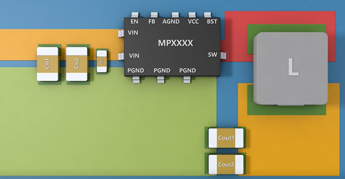
Output Capacitor: Similar to the input capacitor, the output capacitor should be placed close to the output of the inductor VOUT and power ground PGND, with the shortest connection to PGND and copper poured to ensure the power circuit is minimized.
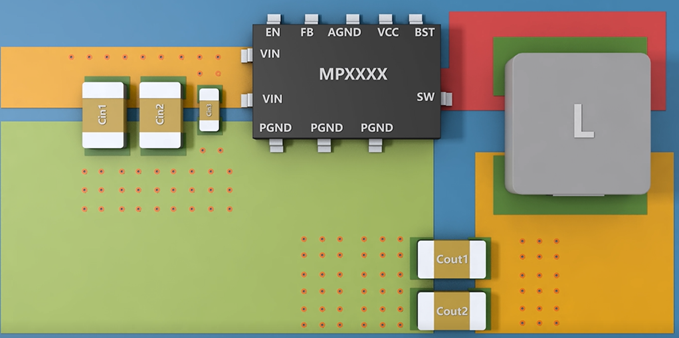
Poured Copper Area and Number of Vias: These two factors affect the PCB current-carrying and heat dissipation capabilities. Generally, it is necessary to increase the number of vias at VIN, Vout, and GND to maximize copper pouring in these areas to reduce parasitic resistance. The copper pouring at the SW point should not be too small to avoid current limiting, which can lead to abnormal operation. The current-carrying capacity of the PCB is related to the board material, thickness, trace width, and temperature rise, which is quite complex and can be accurately determined through specific design specifications.
3. Logic Circuit PCB Layout
In a Buck circuit, attention should generally be paid to the following logic aspects: Bootstrap Capacitor, Feedback Circuit, VCC and Single Point Grounding.
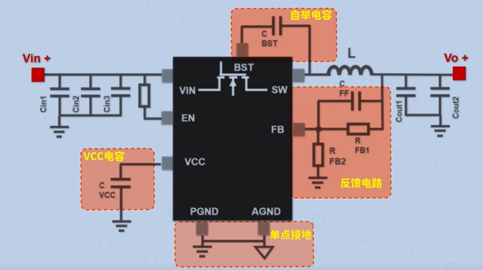
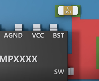
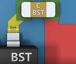
Bootstrap Capacitor: In high-voltage Buck chips, the integrated upper switch is generally an NMOS, thus requiring a BST bootstrap circuit. During the inductor discharging period, charging the bootstrap capacitor generates a voltage higher than SW at the BST pin, driving the upper switch during the inductor charging period. Therefore, BST is also a point of rapid voltage change, radiating strong noise. The bootstrap capacitor should be placed as close as possible to BST and SW, with routing widths generally around 20mil.
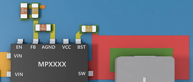
Feedback Circuit: Generally includes FB voltage divider resistors and feedforward capacitors. Since the voltage at the FB point is very low, typically around 0.6-0.8V, it is easily confused with noise or ripple, making it the most sensitive and easily disturbed part of the chip, and a common cause of system instability. Therefore, during routing, the voltage divider resistors and feedforward capacitors should be placed as close to the chip as possible to reduce noise coupling. The routing from the FB resistor to the FB pin should be as short as possible to minimize parasitic inductance and impedance. At the same time, it is important to note that the routing from FB to Vo can be set on other layers through vias, but should also be kept as far away from noise sources as possible, such as SW, BST, inductors, etc.
VCC Capacitor:VCC supplies power to the chip’s logic circuit and is the output of the chip’s internal LDO. The VCC capacitor should be placed close to the chip’s VCC pin and between the GND pins to stabilize the voltage. Additionally, the capacitor should ideally be on the same layer as the chip, without vias.
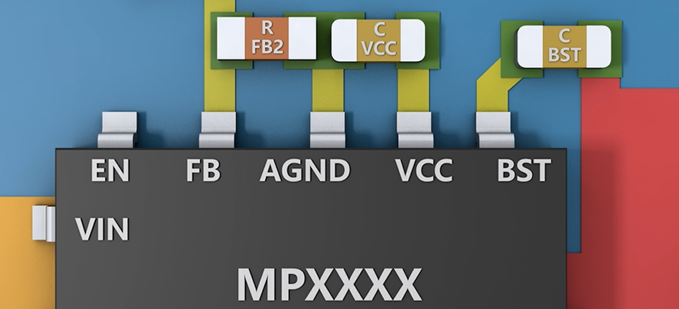
Single Point Grounding: For chips with larger output currents, their grounds are generally divided into PGND and AGND, where PGND is the power ground, and AGND is the signal ground, which is generally associated with FB, EN, VCC and other logic parts of the chip. To prevent the entire power ground from affecting the more sensitive signal ground, it is recommended to connect AGND and PGND at a single point, which can also be done through a 0ohm resistor.
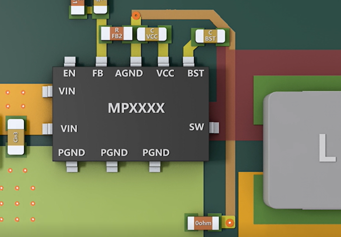
This is because although the large copper area of PGND can absorb noise from the power input, in cases of larger output currents, the noise radiated will still affect sensitive logic circuits. The single point connection routing method can provide a relatively “clean” ground for our logic circuits.
Above are the key points to pay attention to when designing a Buck circuit PCB. When unsure about how to start drawing the PCB, you can also refer to the chip’s specifications, check the demo board’s PCB layout or related guidelines.
4. PCB “Health Check List”
Finally, to help everyone understand whether their drawn PCB is reasonable, you can refer to the following PCB “Health Check List” for self-assessment:
| Design Suggestions | Weight (%) | Self-Assessment Score | Remarks |
| Component Placement | Input capacitors should be placed close to the chip, decoupling capacitors need to be placed next to VIN and power PGND pins within 6mil (minimum spacing allowed), ideally not exceeding 40mil. Place on the same layer as the chip. | 20 | |
| Inductor should be placed close to SW pin. Place on the same layer as the chip. | 15 | If using a power module, this item can be ignored | |
| Output capacitors should be placed close to the inductor Vout end and power PGND. Place on the same layer as the chip. | 15 | ||
| Freewheeling diode needs to be placed close to the inductor SW and power PGND. Place on the same layer as the chip. | 5 | If using a synchronous power chip, this item can be ignored | |
| VCC capacitor should be placed close to the chip’s VCC pin. Place on the same layer as the chip. | 3 | ||
| FB resistor should be placed close to FB pin, with routing as short as possible. Place on the same layer as the chip. Keep away from noise sources. | 3 | ||
| BST RC should be placed close to SW and BST pins. Place on the same layer as the chip. | 3 | ||
| COMP RC should be placed close to the pin. | 3 | If this pin is not present, this item can be ignored | |
| Large power network copper pouring | VIN copper pouring | 3 | |
| SW copper pouring should be as short as possible while ensuring sufficient current flow. | 4 | ||
| Vout copper pouring | 3 | ||
| GND copper pouring | 4 | Overall copper pouring is more convenient to perform at the end | |
| VIA vias |
GND network via count ≥(Iin+Iout)/200mA |
4 | |
|
VIN network via count ≥Iin/200mA |
3 | ||
|
Vout network via count ≥Iout/200mA |
3 | ||
| Vias should not be placed on chip pins or component pads | 1 | ||
| Other weak signal | EN resistor should be placed close to the chip, can be placed on different layers. | 1 | |
| SS RC should be placed as close to the chip pin as possible. | 1 | ||
| PG | 1 | ||
| Others (CS, mode etc.) | 1 | Refer to the corresponding specifications | |
| Routing | Routing and copper pouring should use 45° or rounded corners. | 2 | |
| No routing under the inductor. | 1 | ||
| Sampling signals should be routed in parallel. | 1 | If this function is not present, this item can be ignored |