During the process of troubleshooting circuit faults, if there is no circuit diagram for reference and the fault being handled is relatively complex, it is necessary to draw a circuit diagram based on the actual situation of the components and printed circuit on the PCB.
1. Basic Ideas and Methods for Drawing Circuit Diagrams from PCBs
1. Basic Idea for Drawing Circuit Diagrams
1) Minimize the drawing range as much as possible
There is no need to draw the entire machine circuit diagram. Based on the fault phenomenon and possible inspection steps, the fault can be narrowed down to a minimal range, and only the circuits within this range should be drawn based on the physical components.
2) Identify the type of unit circuit
Determine the type of circuit based on the characteristics of the components on the PCB, for example, whether it is a rectifier circuit in a power supply circuit or an amplifier circuit, thus identifying the general direction of the circuit type.
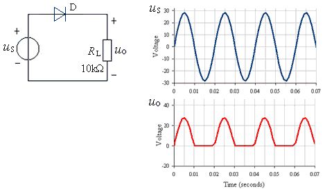
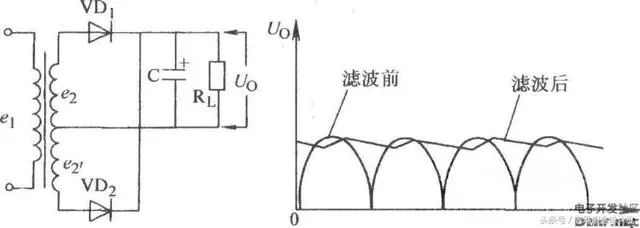
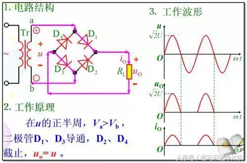
Then, based on the circuit type, observe the characteristics of the components on the PCB to determine the approximate type of specific unit circuits. For example, if a rectifier diode is seen, it is a half-wave rectifier circuit; if two rectifier diodes are seen, it is a full-wave rectifier circuit; if four rectifier diodes are seen, it is a bridge rectifier circuit.
3) Select reference circuits
Based on the specific type of circuit, use the circuits learned as reference circuits. For example, for a full-wave rectifier circuit, first draw a typical full-wave rectifier circuit, then compare it with the actual circuit on the PCB for adjustments.
4) Verification method
After drawing the circuit diagram, perform a reverse check by comparing the drawn circuit diagram with the actual situation on the PCB, that is, verify whether the components in the drawn circuit are correctly connected on the PCB. If there are errors, it indicates that the drawn circuit diagram is incorrect.
2. Simple Method to Observe Copper Foil Circuit Direction on PCB
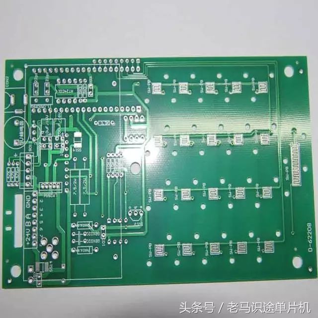
When observing the connections between components and the copper foil circuit on the PCB, a lamp can be used for illumination. Shine the light on the side with copper foil circuits, and it will be clear and convenient to see the connection of the copper foil circuits with each component on the component side, which can save the trouble of flipping the PCB. Constantly flipping the PCB is not only cumbersome but also risks breaking the leads on the PCB.
3. Observing Copper Foil Circuits on Double-Sided PCBs
1) Structure of Double-Sided Boards
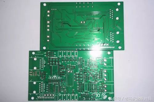
The diagram below is a schematic of a double-sided PCB. Both the component side (top layer) and the back side (bottom layer) have copper foil circuits, and surface-mounted components can be installed on either the top or bottom layer.
2) Via Holes
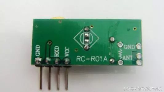
To connect the copper foil circuits on the top and bottom layers, vias are set up on the PCB, as shown in the diagram below. Wherever it is necessary to connect the copper foil circuits on the top and bottom layers, a via will be set up. When drawing, it is necessary to indicate that the via connects the two layers of copper foil circuits.
The diagram below shows an actual double-sided copper foil circuit.
4. Method for Drawing Circuit Diagrams Based on Components
Analyzing the working principle of the circuit, the key is to capture the power supply voltage +V terminal (or -V terminal), ground terminal, signal input terminal, and signal output terminal. When drawing circuit diagrams based on the PCB (since the distribution of the printed circuit on the PCB is often inconsistent with the rules of the circuit diagram), it is necessary to first draw the interconnections between components, and then connect them to their respective terminals. Here, the method will be illustrated using a transistor circuit as an example.
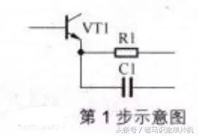
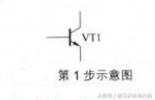
1) Step One
First, draw the circuit symbol for the transistor, as shown in the diagram below. If there are two components, R1 and C1, connected to the emitter of the transistor VT1, all should be drawn.
2) Step Two
After drawing R1 and C1, look for the components or lines connected to the other end of R1 and C1 on the PCB, as shown in the diagram below.
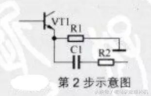
It is found that R1 is connected to the ground, and the ground symbol can be directly drawn. It is also found that C1 is connected to another resistor R2, and the circuit symbol for R2 should be drawn in series with C1.
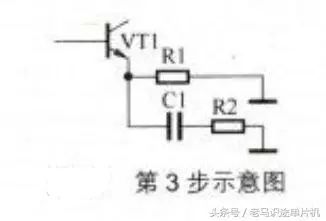
3) Step Three
Continue to find the other end of R2 on the PCB and find the ground line, as shown in the diagram below. Usually, when a component is connected to the ground or the power supply, the drawing of this branch circuit can be concluded.
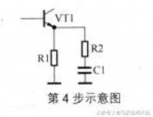
4) Step Four
According to the usual drawing method, organize the drawn sketch, as shown in the diagram below, to facilitate analysis and understanding of this circuit.
2. Methods for Drawing Transistor Circuits
Drawing circuit diagrams based on the actual components on the PCB also has methods and techniques. The key is to be familiar with commonly used circuits of various components, making the drawing process much easier.
1. Method for Drawing Transistor Amplifier Circuits
1) Step One: First, draw the circuit symbol for the transistor.
First, determine whether the actual transistor on the PCB is of NPN or PNP type. The most commonly used is the NPN type transistor, as shown in the diagram below.
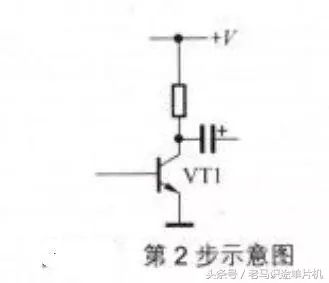
2) Step Two: Draw the collector circuit.
Find the collector of VT1 on the PCB, then draw all components connected to the collector, paying attention to the resistor connected to the power supply circuit. The diagram below shows the collector connected to the DC working voltage +V terminal through a resistor, and note that the coupling capacitor is connected to the next amplifier.
3) Step Three: Draw the emitter circuit.
The components on the emitter of VT1 are generally connected towards the ground, and there are usually many components connected between the emitter and the ground, which could be capacitors or resistors. The diagram below shows a resistor connected.
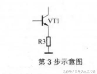
4) Step Four: Draw the base circuit.
The components on the base of VT1 have three directions: towards the power supply, towards the ground, and towards the previous stage circuit.
The diagram below shows R1 in the direction of the power supply +V, while there are usually resistors in the direction of the ground and coupling capacitors in the direction of the previous stage.
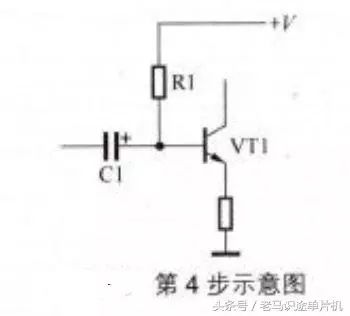
5) Step Five: Draw the entire transistor circuit.
Assemble the circuit diagrams from the above four steps into a complete circuit diagram, as shown in the diagram below. From this circuit, it can be seen that this is a DC circuit of a common-emitter amplifier.
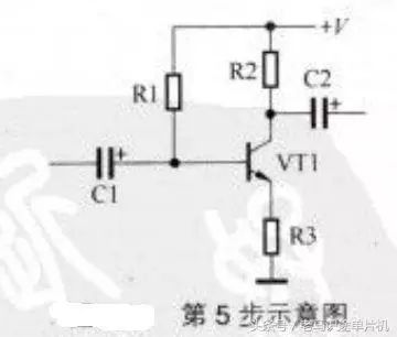
If the drawn circuit does not conform to circuit logic, it is very likely that there is an error in the drawing, but it could also be that this circuit is relatively special.
2. Methods for Drawing Other Transistor Circuits
When drawing other circuits of transistors based on the actual components on the PCB, the key is to understand the general function of the transistor, such as whether it is part of an oscillator circuit or a controller circuit. After determining this general direction, identify the specific type of circuit based on the characteristics of the components.
1) Step One:
Draw the DC circuit of the transistor. In most application circuits of transistors, there is a DC circuit. If during the drawing process it is found that the transistor does not have a complete DC circuit, then this transistor is likely not working in amplification, oscillation, etc., but forms a special circuit, such as a transistor ALC (Automatic Level Control) circuit. Such judgments require solid circuit knowledge.
2) Step Two:
Draw the circuit of the components connected to the three terminals of the transistor.
3) Step Three:
Organize the drawn sketch for easier analysis of the working principle of the circuit. If obvious circuit errors are found during the analysis, it indicates that the circuit diagram is likely incorrect, and verification against the PCB is needed.
3. Methods for Drawing Integrated Circuits
1. Draw the Symbol for Integrated Circuits
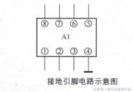
First, clarify how many pins the integrated circuit has based on the physical object, and draw the corresponding symbol for the integrated circuit with the appropriate number of pins, as shown in the diagram below.
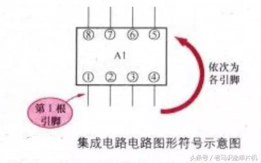
This is a dual in-line integrated circuit with 8 pins, so the circuit symbol should be drawn in a dual-column format with 8 pins, and the pin numbers should follow the general drawing rules, arranged counterclockwise starting from the lower left corner.
2. Draw the Ground Pin Circuit
The method to find the ground pin is: after turning off the circuit, use a multimeter to measure the resistance between that pin and the ground; if the resistance is 0 ohms, then that pin is the ground pin, and a ground symbol should be drawn on that pin, as shown in the diagram below.
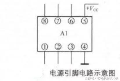
3. Draw the Power Pin Circuit
The method to find the power pin is: under powered conditions, use a multimeter to measure the DC voltage of each pin relative to the ground of the PCB; the pin with the highest voltage is the power pin, and a +Vcc symbol should be drawn on that pin, as shown in the diagram below.
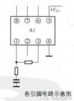
4. Draw the Circuit for Each Pin
The method for drawing the circuit for other pins is: find a certain pin, such as pin 1, and trace all the circuit symbols of the components connected to pin 1 along the copper foil line.
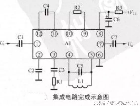
If there are series components in the external circuit of that pin, they should also be drawn one by one until a relatively clear circuit diagram is drawn, such as drawing to the ground or power supply terminal or to another pin of the integrated circuit, as shown in the diagram below.
After drawing the external circuits of each pin of the integrated circuit, organize the circuit diagram, draw it in the usual way, and number the components in the circuit from top to bottom and from left to right, as shown in the diagram below. If necessary, check the models and nominal values of the components based on their physical objects.
Copyright Statement: This article’s copyright belongs to the original author and does not represent the views of the association. Articles pushed by the “Jiangxi Province Electronic Circuit Industry Association” are for sharing purposes only and do not represent the position of this account. If there are copyright issues, please contact us for deletion.