IntroductionRecently, some friends have reported that they did not understand the power supply circuit of our open-source Bluetooth speaker solution. Open-source address: https://oshwhub.com/sunsilicon/s-be5607eThe power supply design of the Bluetooth System-on-Chip (SoC) is crucial, directly affecting the performance, stability, battery life, and cost of Bluetooth devices. When designing, multiple aspects must be considered comprehensively to ensure that the power supply system can stably and efficiently power the Bluetooth SoC.Overview of S-BE5607E Power SupplyThe power management unit (PMU) characteristics are as follows:
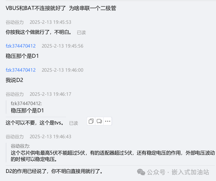
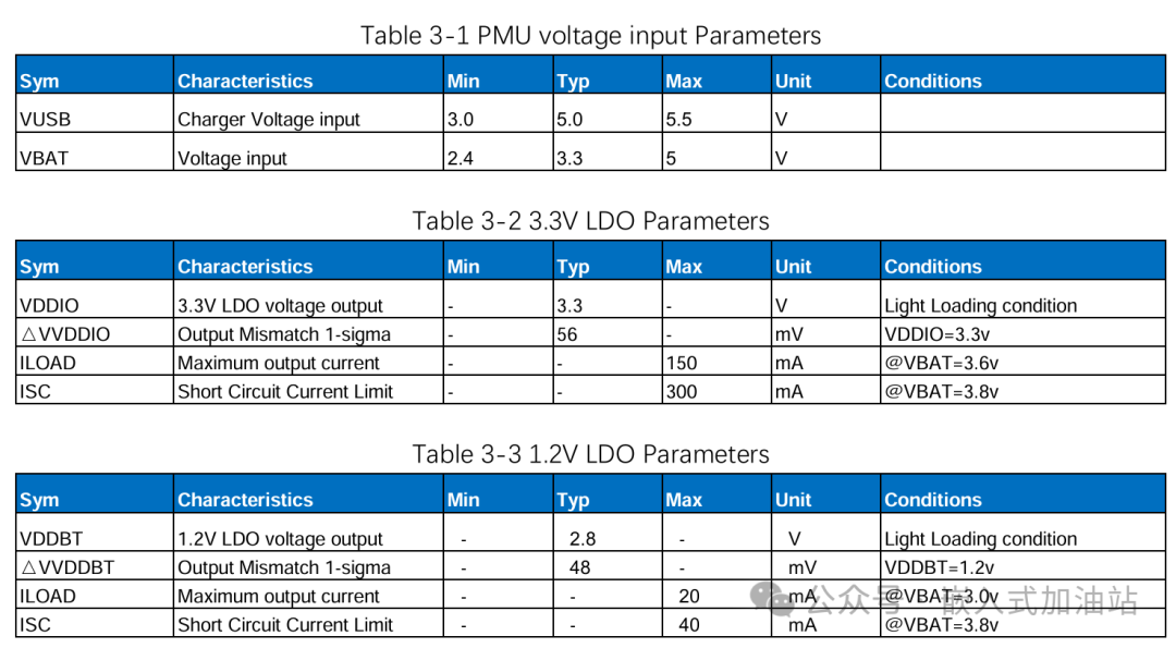 The power supply pin of S-BE5607E is pin 15 (VBAT), with a voltage range of 2.4~5V. Note that the maximum is 5V and must not exceed 5V. Some friends have expressed confusion about why D2 is needed in a USB-5V power supply system. Generally, mobile phone chargers or nominal 5V power adapters have an output voltage range of 4.75~5.25V, and the voltage will exceed 5V when unloaded or lightly loaded. A voltage exceeding 5V on pin 15 (VBAT) can damage the chip. D2 also serves to stabilize the voltage of the S-BE5607E IC; when external voltage fluctuates, D2 can prevent the voltage of capacitor C9 from being pulled down, forming a PI-type filter circuit with C8 and R8 to stabilize the power supply voltage for the Bluetooth IC.
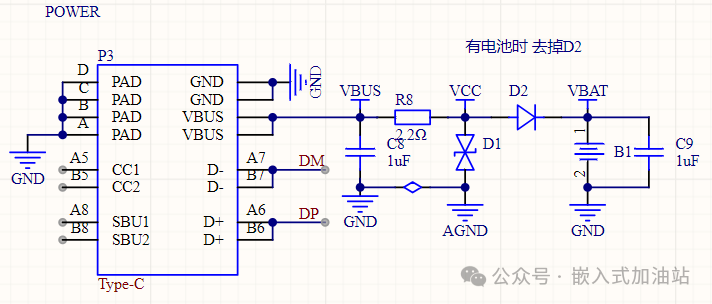
 If you haven’t looked at the specifications or notes, you might think that pin 13 (VUSB) is the power supply pin for the S-BE5607E. In battery-powered Bluetooth headsets or Bluetooth speaker circuits, pin 13 (VUSB) can be used for built-in charging, with a maximum charging current of 350mA and an input voltage not exceeding 5.5V. Due to the small charging current, it is generally used in Bluetooth headsets or speakers powered by small capacity batteries, where R8 can be changed to 0 ohms or a fuse can be used, and D2 can be removed. For Bluetooth headsets or speakers powered by large capacity batteries, please use external power supply.
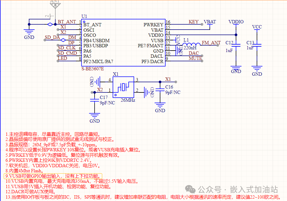 Pin 13 (VUSB) can also serve as a GPIO input/output, but it does not have pull-up or pull-down functionality. It can even be used as a TX pin for UART or RX and TX pins for HSRTX (high-speed serial).When using pin 13 (VUSB) as GPIO or UART, C13 can be omitted.
 Pin 14 (VDDIO) is the internal LDO output pin, used to power peripherals such as LEDs, SD cards, TF cards, microphones, infrared receivers, etc.(For MIC circuit design, please refer to: 【Bluetooth Development Notes】 Analysis of MIC Circuit Design for Bluetooth Speakers and Headsets)
 The voltage range for pin 14 (VDDIO) is 2.8~3.8V, and the voltage value can be programmed. Our standard program sets the voltage to 3.1V. Many friends often ask if C12 can be omitted when not using peripherals like LEDs, SD cards, TF cards, or infrared receivers. The answer is no, because the internal peripherals of the IC, such as DAC, ADC, internal Flash, RF circuits, etc., all require power decoupling from the internal LDO. Otherwise, strange issues may occur, such as noise or failure to program.Many strange circuit phenomena are often caused by poorly designed power supply circuits for the IC.About Power Decoupling
Power decoupling (also known as bypassing) is crucial in the power supply design of Bluetooth SoCs to ensure stable operation and enhance overall performance. It can eliminate interference signals from the power supply and reduce the impact of power noise on the Bluetooth SoC. Below is a detailed introduction to its functions and implementation methods:
- Function of Power Decoupling
- Suppressing Power Noise PropagationWhen the Bluetooth SoC is operating, various noises are generated on the power line, which may originate from external power fluctuations or internal circuit switching. Power decoupling can effectively prevent these noises from propagating through the power network, avoiding interference with the normal operation of the Bluetooth SoC. In Bluetooth devices, high-frequency noise is generated when the RF circuit operates; if not decoupled, this noise can propagate through the power line to the digital circuit, affecting digital signal processing and leading to errors or instability in Bluetooth data transmission.
- Stabilizing Power VoltageThe current demand of the Bluetooth SoC varies significantly under different operating modes, which can cause voltage fluctuations. Power decoupling provides a stable power voltage, ensuring that the Bluetooth SoC can operate normally under various working conditions. When the Bluetooth SoC switches from standby mode to data transmission mode, the current suddenly increases, and the decoupling capacitor can promptly supply charge to maintain stable power voltage, preventing abnormal operation of the chip due to voltage fluctuations.
- Improving System Anti-Interference CapabilityBy removing noise from the power supply, power decoupling enhances the anti-interference capability of the Bluetooth SoC system, reducing the impact of external interference on Bluetooth communication, and improving the reliability and stability of Bluetooth devices. In complex electromagnetic environments, well-decoupled Bluetooth SoCs can better resist external electromagnetic interference, maintaining stable communication.
- Capacitor DecouplingThis is the most commonly used method for power decoupling. Near the power pins of the Bluetooth SoC, multiple capacitors of different values are usually placed. Ceramic capacitors, due to their low equivalent series resistance (ESR) and good high-frequency characteristics, are commonly used to filter out high-frequency noise, typically ranging from 0.1μF to 10μF; electrolytic capacitors have larger capacitance and can filter out low-frequency noise and provide instantaneous large currents, with common values ranging from 1μF to 100μF. In practical design, a 0.1μF ceramic capacitor and a 10μF electrolytic capacitor are usually placed in parallel next to the power pins of the Bluetooth SoC to effectively filter out high-frequency and low-frequency noise, respectively.
- Inductor DecouplingInductors have the property of suppressing high-frequency currents. By placing an inductor in series in the power path, high-frequency noise can be blocked. Placing a small inductor in series on the power input line of the Bluetooth SoC can effectively prevent high-frequency interference signals from external power sources from entering the chip. An LC filter circuit composed of inductors and capacitors can further enhance the decoupling effect; in some Bluetooth SoC designs with high requirements for power noise, LC filter circuits are often used for power decoupling.
- Multi-layer PCB DesignA reasonable multi-layer printed circuit board (PCB) design can also achieve power decoupling. In multi-layer PCBs, dedicated power and ground layers are set up, and they are kept closely adjacent to utilize inter-layer capacitance for decoupling. Increasing the copper foil thickness of the power and ground layers reduces the resistance and inductance between power and ground, lowering power noise. Additionally, during PCB routing, it is essential to ensure that the power path is short and wide to reduce line impedance and improve decoupling effectiveness. The power pins of the Bluetooth SoC should be placed as close as possible to the power and ground layers to shorten the power path and reduce noise generation.
- Power Plane SegmentationFor Bluetooth SoC systems with multiple power voltages, using power plane segmentation technology can avoid mutual interference between different power supplies. By separating power planes of different voltages and using capacitors for decoupling at the segmentation points, noise coupling between different power supplies can be prevented. In a Bluetooth SoC design with both 1.8V and 3.3V power supplies, effectively reducing interference between the two power supplies can be achieved by segmenting the 1.8V and 3.3V power planes and placing multiple decoupling capacitors at the segmentation points.
The power supply for S-BE5607E uses capacitor decoupling, selecting high-quality 1uF MLCC capacitors.
Layout Considerations
1. Decoupling capacitors should be placed as close to the main control as possible, with short loop paths and minimal loop area;
2. Pay attention to thick wiring in the charging circuit to ensure that large currents pass through without heating.
Thank you for watching. If you need materials, please leave a message in the comments. Or check the original text for downloads.Original content is not easy to create, please use your wealth to help the editor like and give a thumbs up to the article. Welcome to follow for more exciting content delivered in a timely manner!
Thank you again for your reading. The author has limited abilities, and mistakes are inevitable, so please criticize and correct!
Previous HighlightsVC-S100D-CW Smart Offline Voice Recognition Warm and Cool Color Monochrome Night Light IC SolutionIntroducing a Cost-Effective Zigbee Wireless ModuleNXP Zigbee JN516X JN517x JN518X Development and Compilation in vsCode Studio EnvironmentRecommended vsCode Plugin for Intelligent Code Generation, Code Completion, Code Explanation, and Code Correction: iFlyCodeI wrote a low-cost smart voice-controlled night light solution, searched in AI, and found that AI summarized it very well, understanding my design better than I do.[Solution Recommendation] Guangming Valley Launches VC-S100D Cost-Effective Voice-Controlled Night Light SolutionGuangming Valley S-BE5607E Bluetooth 5.4 Low-Cost Card/USB/Bluetooth Speaker Solution[Solution Recommendation] SMP37A-Player Low-Cost Card/USB/USB Speaker/MP3 Playback/USB Sound Card SolutionBased on SUN6200 Wireless Communication Module C51 Example Program SDK Open Source Code InterpretationZhongsu Lanyun AB5607E Bluetooth 5.4 Low-Cost Bluetooth Proximity Switch Timer Solution[Application Solution] Based on MT7628 JN5169-Zigbee-4G Smart Gateway Solution[Recommended Good Product] Stickman Privacy Camera AI Smart Behavior Detection Fall Alarm[OpenWRT] MT7628/7688 OpenWRT UART2 GuideSmart Offline Voice Recognition Whole House Smart Voice Control SolutionMillimeter Wave Radar S-ED713 AI Smart Sleep Monitor Sleep Quality Analysis Vital Sign DetectionA Menu Framework for Microcontrollers Written Using Linked Lists: MCU Menu FrameEC20 DialSolution for No URC Reporting During CallsZhongsu Lanyun Development Program Download and Debugging MethodsHow to Simulate and Offline Program the Jinrui Microcontroller?
NXP Zigbee JN5169 Development Environment Software Documentation and Support Resources Pack Download
[Application Note] BK3432 BLE Clock and Power Supply Configuration
BK3432_SDK BLE Broadcast Packet Explanation and Code Configuration
BK3432 Typical Application Circuit Hardware Reference Design PCB Layout Guide
[Recommended] BK3432 Dual-Mode BLE5.0 Classic Dual-Mode Bluetooth SoC Chip QFN32 Package
The AI function of the public account has been upgraded again, finding solutions, materials, and writing code technical issues are all easy!Analysis of Crystal Oscillator Circuit Design Based on Bluetooth SoC
Complete Analysis of Bluetooth Protocol: Understand the Bluetooth Protocol in One Article