This article is a featured article from the Kanxue ForumAuthor of Kanxue ForumID: Hu Yimi
In this article, we share some research content about the Loock Touch smart lock, which is produced by Yunding Technology. Yunding Technology is a company focused on the research and production of smart home security products, with two major brands: “LuKe” for the home market and “Yunding” for the apartment market.
Loock Touch is one of the flagship products of the LuKe brand, and its architecture is very similar to that of the D2 and D3 smart locks under the Yunding brand. The latest flagship product of LuKe is the Loock Touch 2 Pro, which has a hardware architecture that is quite different from all previous products.
Since the Fat Monkey Lab has always had a good cooperative relationship with Yunding Technology, the following analyses and discussions will focus only on the analytical methods and research processes, without involving any details related to vulnerabilities, similar to the previous article about Hikvision’s EZVIZ smart gateway.
2.1 Unlocking Process Analysis
In a previous article, we analyzed the Guojia smart lock, link: https://bbs.pediy.com/thread-259530.htm. In this analysis, we will also analyze from the perspective of BLE unlocking. The Loock Touch lock from Yunding LuKe can also be unlocked directly via BLE from a mobile phone, so we will start the analysis from the app’s unlocking process.
The app downloaded from the application market for the Yunding LuKe smart lock is wrapped with a Baidu Enterprise version shell. After unwrapping, we can see the logs printed by the app (unwrapping is not within the scope of this series of articles, and analyzing the iOS version is also possible). After operating the phone to unlock the door, we found several log entries in the app’s logs that attracted our attention.
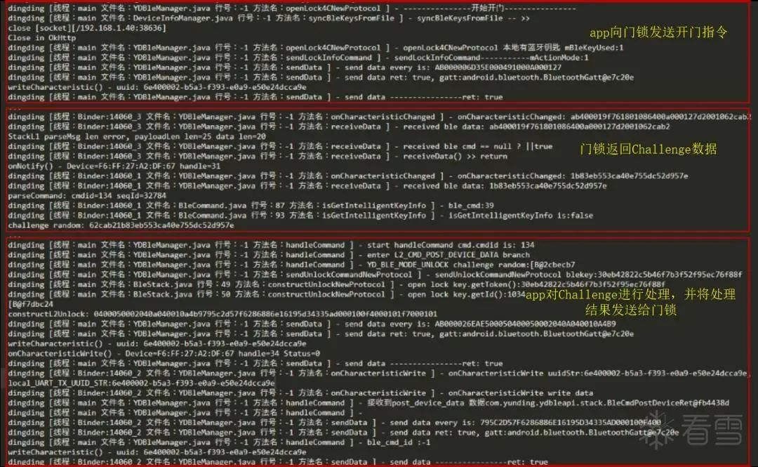
Figure 2-1 Logs printed by the app during unlocking
Based on the contents of the three red boxes in the above figure, we can infer that the unlocking process is authenticated based on a Challenge/Response model, with the specific process as follows:
(1) After the app establishes a BLE connection with the lock, when using the app to unlock the door, the app first sends a notification command to inform the lock to prepare to enter the unlocking process;
(2) The lock then sends a set of numbers to the phone, called Challenge;
(3) The app processes the Challenge to generate a Response and sends it back to the lock. When the lock verifies that the Response is correct, it will unlock.
We compared the app logs during multiple unlock attempts and found that the notification command sent in step (1) each time only had one byte of content that was different, as shown in the following figure:
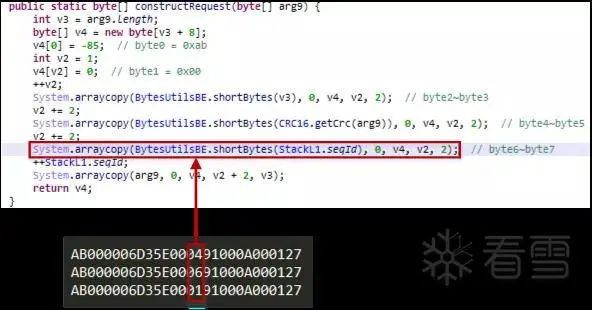 Figure 2-2 Comparison of notification commands
In the above figure, we compared three notification commands and found that only the 7th byte was different. In the code segment where the app encapsulates the data packet, we can determine that this byte represents seqID, which is the sequence number of the data packet. Therefore, we can infer that this notification command functions similarly to the SYN packet in the TCP protocol, serving only to establish a handshake, while the lock’s authentication process for the phone mainly relies on steps (2) and (3). Next, we will analyze how the app processes the Challenge and generates the Response.
2.2 Processing of Challenge
2.2.1 Challenge Processing Flow Analysis
By searching for log content in the code, we can determine that after receiving the Challenge data, the app processes it using the method shown in the following figure.
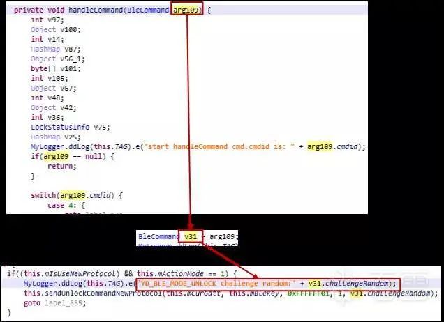 Figure 2-3 Challenge data processing
In the figure, the handleCommand method is used to process the BLE returned data, and the Challenge returned by the lock is passed as a parameter to the method sendUnlockCommandNewProtocol. Based on the parameters and method name, this is the method for processing Challenge data, generating the Response, and sending it back to the lock.
Further examination of the code reveals that in the sendUnlockCommandNewProtocol method, the encryptBleKeyNewProtocol method is ultimately called to process the Challenge data. The data returned from this method, after adding a header, will be directly sent to the lock.
Figure 2-3 Challenge data processing
In the figure, the handleCommand method is used to process the BLE returned data, and the Challenge returned by the lock is passed as a parameter to the method sendUnlockCommandNewProtocol. Based on the parameters and method name, this is the method for processing Challenge data, generating the Response, and sending it back to the lock.
Further examination of the code reveals that in the sendUnlockCommandNewProtocol method, the encryptBleKeyNewProtocol method is ultimately called to process the Challenge data. The data returned from this method, after adding a header, will be directly sent to the lock.
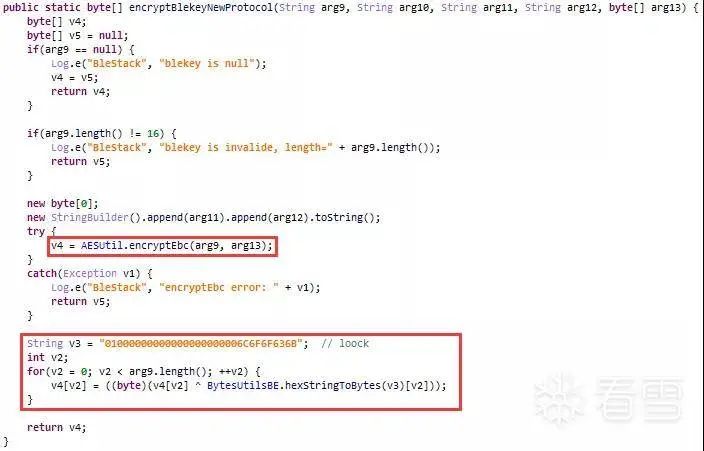 Figure 2-4 Encrypting Challenge data
In the figure, the parameter arg13 is the Challenge data. It can be seen that the AES EBC encryption is used in this method, with the key being parameter arg9. After encryption, the ciphertext is XORed with a fixed data set.
From the above analysis, we can infer that in the unlocking process, the lock’s authentication of the phone relies on the AES EBC algorithm shown in Figure 2-3, meaning that both parties use the same key to encrypt and decrypt the Challenge. Only when the phone possesses the correct AES key can it pass the authentication to unlock the door. Therefore, the security of the unlocking process depends on whether the keys used by the lock and the phone are secure.
2.2.2 Obtaining the Challenge Encryption Key
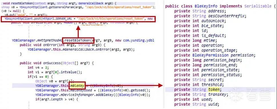
In Figure 2-3, the encryption key is parameter arg9. By tracing back arg9, we can determine that the key used to encrypt the Challenge is obtained through the resetBleToken method, as shown in the following figure.
Figure 2-5 Obtaining the encryption key
In the resetBleToken method, an HTTP request is sent. After processing the returned BleToken, some variables are assigned values. In the figure, mBleKey is a variable of type BleKeyInfo, and its token member variable is the encryption key for the Challenge data described in section 2.2.1. In the following text, we will refer to this encryption key as BleKey.
From the above analysis, we can conclude that the BleKey is requested by the app from the server, which leads to two possibilities:
(1) Every time the app establishes communication with the lock, it requests a Key and sends it to the lock;
(2) When the app establishes communication with the lock, it only sends a request to the server if there is no available BleKey.
To verify the above assumptions, we repeatedly unlocked the door multiple times with the phone, establishing communication between the phone and the lock. During this process, we did not find any requests or related content in the app logs or the captured data packets, leading us to conclude that the app likely stores the BleKey locally and does not need to obtain it from the server.
We can delete the locally stored BleKey by clearing the app’s cache. After deletion, the logs during the app unlocking process changed, as shown in the following figure:
Figure 2-6 Logs after deleting the app’s Bluetooth key
By comparing the logs in Figures 2-6 and 2-1, we can see that after deleting the BleKey, the app first executed resetBleToken when unlocking the door, which aligns with our analysis.
We also noticed that after resetBleToken, there is another log entry sendBleKeyCommandNewProtocol, which is the method for sending the BleKey to the lock. We will analyze the process of the phone obtaining the BleKey in section 2.2.4, while the process of the phone sending the BleKey to the lock will be analyzed in section 2.2.4.
Meanwhile, we also captured the corresponding HTTP request in Fiddler, as shown in the following figure:
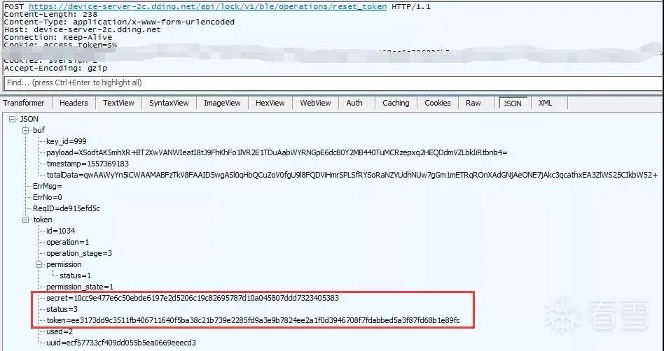 Figure 2-7 reset_token request
After receiving the returned BleToken, the app will use the AES CBC algorithm to decrypt the secret and token shown in the red box in the above figure. The relevant code is shown in the following figure:
Figure 2-7 reset_token request
After receiving the returned BleToken, the app will use the AES CBC algorithm to decrypt the secret and token shown in the red box in the above figure. The relevant code is shown in the following figure:
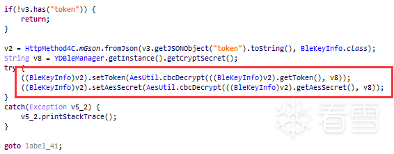 Figure 2-8 Processing of the reset_token return value
At this point, it can be confirmed that the BleKey obtained by the app from the server is also saved using the AES CBC encryption algorithm. From Figure 2-8, we can see that its key is returned by the getCryptSecret method. We will now analyze the source of the CryptSecret.
Figure 2-8 Processing of the reset_token return value
At this point, it can be confirmed that the BleKey obtained by the app from the server is also saved using the AES CBC encryption algorithm. From Figure 2-8, we can see that its key is returned by the getCryptSecret method. We will now analyze the source of the CryptSecret.
2.2.3 Obtaining CryptSecret
The key used to decrypt the BleKey is obtained through the getCryptSecret method. Therefore, we can start from this method, and the relevant code search results are shown in the following figure.
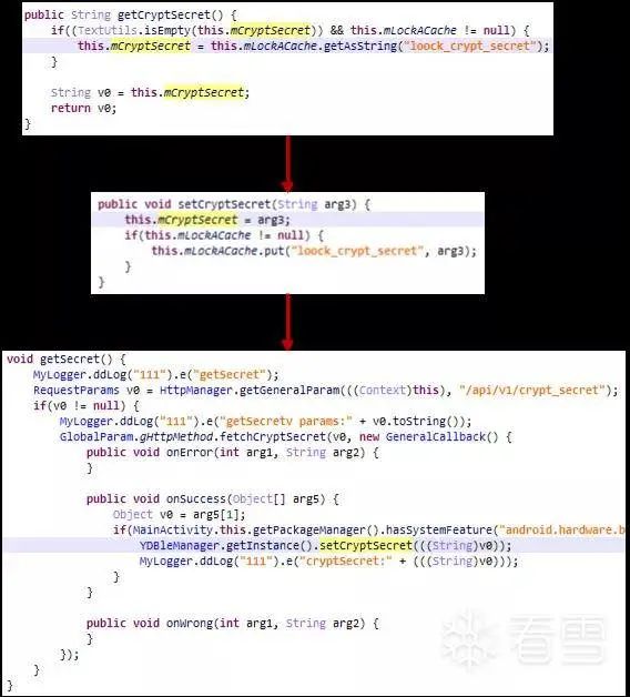 Figure 2-9 Code flow for obtaining CryptSecret
In the figure, the getCryptSecret method returns this.mCryptSecret, and this variable is assigned a value through the setCryptSecret method, which is called in the getSecret method.
In the getSecret method, it can be seen that the CryptSecret is obtained from the Yunding LuKe server, with the URL being “api/v1/crypt_secret”. Similarly, we can also capture the crypt_secret data packet in Fiddler, as shown in the following figure:
Figure 2-9 Code flow for obtaining CryptSecret
In the figure, the getCryptSecret method returns this.mCryptSecret, and this variable is assigned a value through the setCryptSecret method, which is called in the getSecret method.
In the getSecret method, it can be seen that the CryptSecret is obtained from the Yunding LuKe server, with the URL being “api/v1/crypt_secret”. Similarly, we can also capture the crypt_secret data packet in Fiddler, as shown in the following figure:
 Figure 2-10 crypt_secret request and response
Since some of the information here is sensitive, we have blurred it out.
2.2.4 Sending BleKey to the Lock
As mentioned in section 2.2.2, the sendBleKeyCommandNewProtocol function is responsible for sending the BleKey to the lock. The function is shown in the following figure:
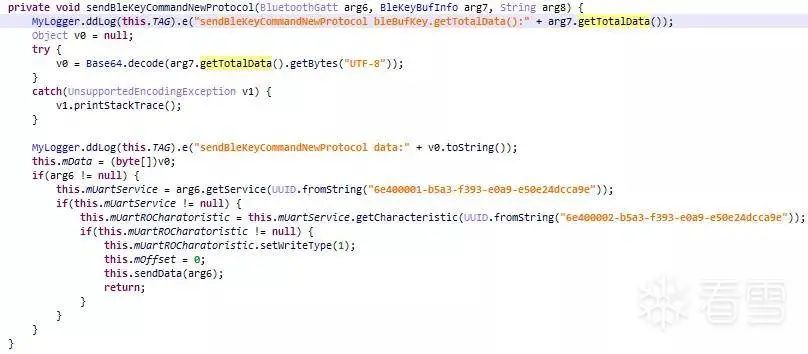 Figure 2-11 Function for sending BleKey from phone to lock
Combining the above figure with the logs from Figures 2-6 and 2-7, we can see that the process of sending the BleKey from the phone to the lock is very simple: it involves base64 decoding the totalData in the reset_token return data packet, and the decoded binary data is sent directly to the lock via BLE communication. The processing of totalData by the lock will be analyzed in subsequent articles.
Figure 2-11 Function for sending BleKey from phone to lock
Combining the above figure with the logs from Figures 2-6 and 2-7, we can see that the process of sending the BleKey from the phone to the lock is very simple: it involves base64 decoding the totalData in the reset_token return data packet, and the decoded binary data is sent directly to the lock via BLE communication. The processing of totalData by the lock will be analyzed in subsequent articles.
2.3 Summary of the App Unlocking Process
After the analysis in Chapter 2, we can summarize the unlocking process of the Loock Touch lock as shown in the following figure.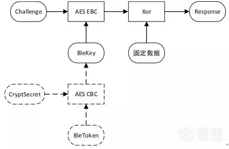 Figure 2-12 Unlocking process diagram
In the above figure, the unlocking process can be divided into two parts:
(1) The dashed part indicates that when the app does not have an available BleKey stored, it will request two sets of data, CryptKey and BleToken, from the server. By using CryptSecret as the key, the data in BleToken is decrypted using AES CBC, which allows us to obtain the BleKey.
(2) The solid part indicates that when the app has an available BleKey, it will use the BleKey as the key to encrypt the Challenge using AES EBC. After XORing the ciphertext with a fixed data set, it serves as the main content of the Response sent to the lock. The lock will only unlock if the Response is successfully verified.
In the previous text, we focused on how the mobile end processes and sends BLE messages. Next, we will look at how the lock processes BLE messages.
3.1 Debugging Interface and Debugger
In previous articles, we have introduced the method of debugging Hikvision’s EZVIZ firmware program through gdbserver, link: https://bbs.pediy.com/thread-261679.htm. Typically, gdbserver is a debugging program running in a Linux system environment, utilizing the debugging interfaces provided by the Linux system to complete debugging work without requiring much hardware assistance.
However, in certain scenarios, such as when there is no Linux operating system, tools like gdbserver cannot meet our debugging needs. In this case, we need to directly use the hardware debugging interfaces and functions provided by the MCU to complete debugging work. By reading the MCU’s chip manual, we can find detailed information about the debugging methods and debugging pins provided by the MCU.
To use the MCU’s debugging interface, we also need a corresponding hardware debugger. Similar to debugging software like IDA and GDB, a hardware debugger allows us to fully grasp the execution status of the debugged program. Generally, hardware debuggers connect to the PC host via USB, and there are many types of communication interfaces between the hardware debugger and the MCU. Different MCUs support different interfaces, and specific information needs to be checked in the manuals of each chip.
The Loock Touch lock we are studying uses the MCU model EFM32GG280F512. By flipping through the chip manual, we can find its debugging interface information as shown in the following figure:
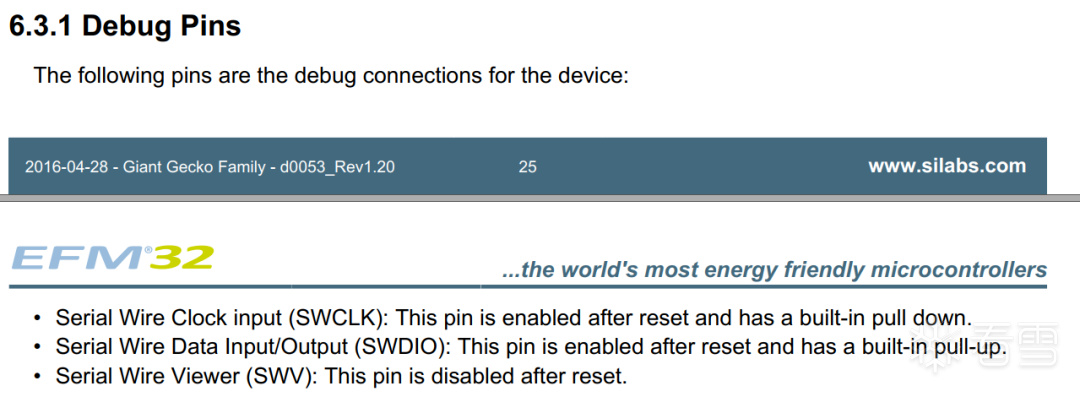 Figure 3-1 EFM32 debugging interface
The debugging interface in the figure is called the SWD interface. Common hardware debuggers that use the SWD interface include JLink and STLink.
The debugger we are currently using, SEGGER JLink (hereinafter referred to as JLink), supports both JTAG and SWD debugging interfaces. During actual use, we only need to connect to the corresponding pins, as shown in the following figure:
Figure 3-1 EFM32 debugging interface
The debugging interface in the figure is called the SWD interface. Common hardware debuggers that use the SWD interface include JLink and STLink.
The debugger we are currently using, SEGGER JLink (hereinafter referred to as JLink), supports both JTAG and SWD debugging interfaces. During actual use, we only need to connect to the corresponding pins, as shown in the following figure:
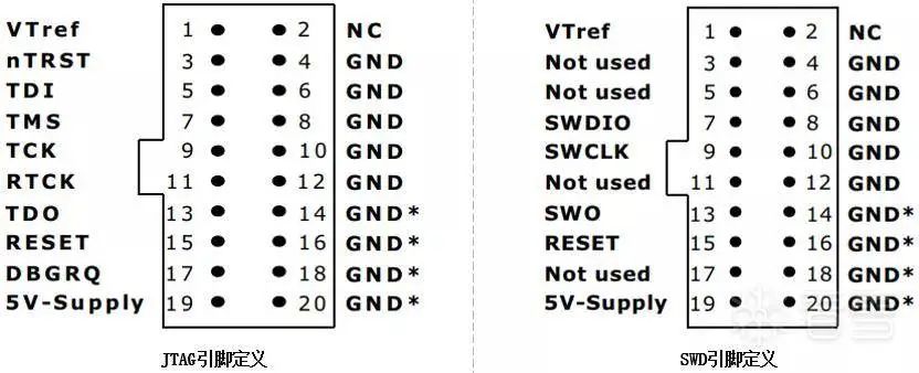 Figure 3-2 Pin definitions of SEGGER JLink
3.2 Extracting Firmware via Debugging Interface
The JLink debugger can read and write the built-in Flash of the chip via the debugging interface, thereby obtaining the complete firmware. Not all chips can extract firmware through the debugging interface; many devices have enabled Readout Protection mechanisms in the release version, preventing us from reading the Flash content through the debugging interface. Fortunately, the device discussed in this article does not have this mechanism enabled.
Next, we will look for and attempt to connect the JLink to the chip’s debugging interface.
3.2.1 Connecting to the Debugging Interface
On the lock’s circuit board, next to the main control MCU, there is a row of vias. We have already soldered a header pin to this row of vias, as shown in the following figure:
 Figure 3-3 MCU and its interface pins
In the figure, the left red box contains the header pins we soldered, and the circuit board labels the corresponding MCU pin names. After measuring with a multimeter, we can confirm that the IO and CLK pins in the red box are the SWDIO and SWCLK pins of the chip. We mentioned that these two pins are part of the SWD debugging interface. We will connect these pins to the JLink debugger as shown in the following figure.
Figure 3-3 MCU and its interface pins
In the figure, the left red box contains the header pins we soldered, and the circuit board labels the corresponding MCU pin names. After measuring with a multimeter, we can confirm that the IO and CLK pins in the red box are the SWDIO and SWCLK pins of the chip. We mentioned that these two pins are part of the SWD debugging interface. We will connect these pins to the JLink debugger as shown in the following figure.
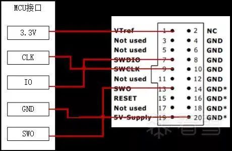 Figure 3-4 Connection of debugging interface to JLink
In the figure, the left side shows the header pins from Figure 3-1, and the right side shows the pins of the SEGGER JLink. After completing the connection, connect the JLink to the USB port of the computer and open the JLink Commander command line tool (relevant tools and user manuals for JLink can be downloaded from SEGGER’s official website: https://www.segger.com/downloads/jlink/). Execute the command shown in the following figure:
Figure 3-4 Connection of debugging interface to JLink
In the figure, the left side shows the header pins from Figure 3-1, and the right side shows the pins of the SEGGER JLink. After completing the connection, connect the JLink to the USB port of the computer and open the JLink Commander command line tool (relevant tools and user manuals for JLink can be downloaded from SEGGER’s official website: https://www.segger.com/downloads/jlink/). Execute the command shown in the following figure:
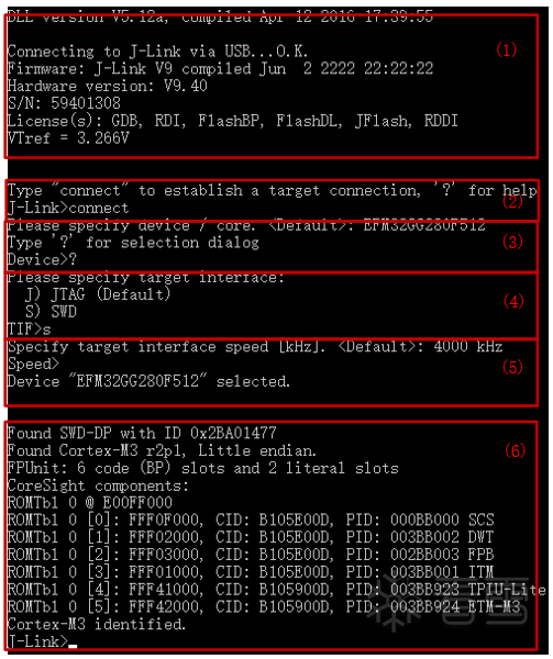 Figure 3-5 Using JLink to connect to SWD interface
Now, let’s explain the contents of the six red boxes in the above figure one by one:
(1) When the command line tool is opened, it first checks the status of the JLink (the JLink from SEGGER’s official website is not ideal in terms of price or delivery time, so we chose a product from a certain treasure; judging by the JLink firmware information printed here, it seems to be a counterfeit product);
(2) Enter the connect command to control the JLink to start connecting to the MCU via the debugging interface;
(3) Enter the ? command to select the chip model to be debugged. In the pop-up dialog, we select the options as shown in the following figure based on the chip’s manufacturer and model;
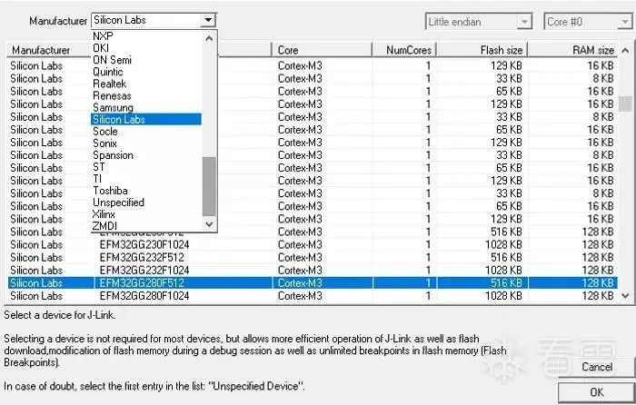 Figure 3-6 Selecting chip model
(4) Enter the s command to select the debugging interface type as SWD;
(5) Choose the communication rate for the interface, generally keeping it at the default setting;
(6) When the content in the sixth red box appears, it indicates that JLink has connected to the MCU via the SWD interface, and we can then read the firmware or perform debugging.
3.2.2 Extracting Firmware
As mentioned earlier, the debugger can read and write the built-in Flash of the chip, and the firmware code is stored in the chip’s built-in Flash. Therefore, we only need to read and save the data in the code storage area, which allows us to obtain the firmware.
Following the approach we used when analyzing the Guojia lock, we can determine from the chip manual that the code is stored in the memory address range of 0x0~0x100000. We will use the savebin command of the JLink Commander command line tool (the usage of this command can be found in the JLink manual) to save the binary data from this area.
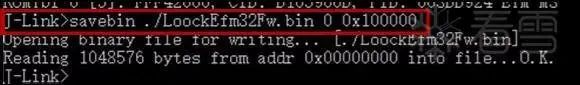 Figure 3-7 Reading binary data of the firmware
In the figure, we obtained the firmware code and named it LoockEfm32Fw.bin.
Figure 3-7 Reading binary data of the firmware
In the figure, we obtained the firmware code and named it LoockEfm32Fw.bin.
3.2.3 Analyzing the Firmware
After obtaining the firmware, we need to parse and reverse engineer it. By consulting the manual, we can see that the core of the EFM32GG280 is the ARM Cortex-M3, which belongs to the Cortex-M series, just like the STM32L0 used in the Guojia lock. Therefore, we can configure IDA and load the firmware using the methods described in the relevant chapters on the Guojia lock.
After loading, we will continue using the approach taken during the Guojia lock analysis to look for the interrupt service routine for the Reset interrupt, which is the data at offset 0x4. After jumping, press the “c” key, and IDA will automatically start parsing the code, as shown in the following figure:
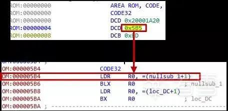 Figure 3-8 Parsing code from the Reset interrupt
As mentioned earlier, the code is stored in the memory address range of 0x0~0x100000, so the base address of the firmware in Figure 3-6 is 0x0. Previously, when analyzing the Guojia lock, the base address when loading the firmware into IDA was 0x08000000, because in the Guojia case, the starting address of the code storage area is 0x08000000. Thus, we successfully extracted and parsed the firmware of the Loock Touch lock.
Figure 3-8 Parsing code from the Reset interrupt
As mentioned earlier, the code is stored in the memory address range of 0x0~0x100000, so the base address of the firmware in Figure 3-6 is 0x0. Previously, when analyzing the Guojia lock, the base address when loading the firmware into IDA was 0x08000000, because in the Guojia case, the starting address of the code storage area is 0x08000000. Thus, we successfully extracted and parsed the firmware of the Loock Touch lock.
3.3 Debugging the Firmware via Debugging Interface
3.3.1 Debugging Features of SEGGER JLink
Before debugging, let’s briefly introduce how to use the debugging features of SEGGER JLink (hereinafter referred to as JLink). In the previous article, we used the command line tool of JLink to extract firmware. This command line tool also includes commands needed for dynamic debugging, such as setting breakpoints, pausing the CPU core, reading/writing registers or memory at specified locations, and single-step debugging.
Specific information can be found in SEGGER’s Wiki (https://wiki.segger.com/J-Link_Commander). One can choose to use openOCD in conjunction with JLink for debugging, but we will not introduce openOCD in this article and will instead choose another debugging tool.
In actual debugging, the command line tool usually needs to be used in conjunction with IDA, which can be very cumbersome and not very intuitive in terms of information display. SEGGER provides a graphical interface tool called Ozone, which can alleviate these issues to some extent. For an introduction to Ozone, please refer to SEGGER’s official website (https://www.segger.com/products/development-tools/ozone-j-link-debugger/), where the software and user manual download page can also be found. The installation of the downloaded software is straightforward.
After installation, you can create a new project through the “File->New->New Project Wizard” option. During creation, you need to select the model of the chip to be debugged, the type of debugging interface, the communication rate, and other information.
Next, click “Debug->Start Debug Session->Attach to Running Program” to connect to the device to be debugged. Note that throughout the debugging process, the computer, debugger, and device need to remain connected, as shown in the following figure.
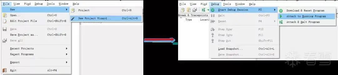 Figure 3-9 Connecting to the device
After connecting to the device to be debugged, Ozone can display multiple subviews, similar to IDA, allowing for simultaneous observation of various information. The following figure shows the debugging interface during one of my debugging sessions.
Figure 3-9 Connecting to the device
After connecting to the device to be debugged, Ozone can display multiple subviews, similar to IDA, allowing for simultaneous observation of various information. The following figure shows the debugging interface during one of my debugging sessions.
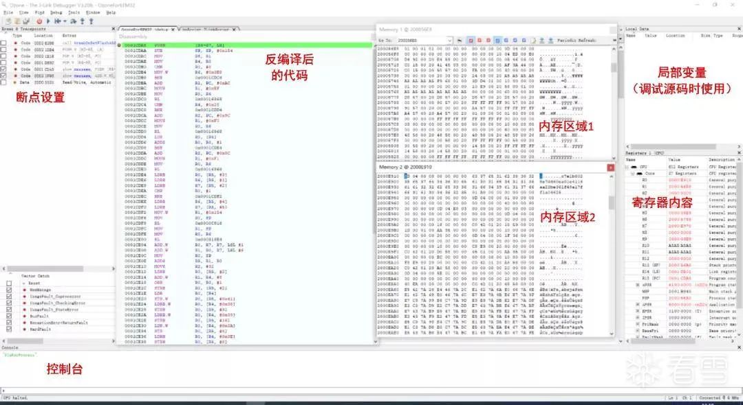
Figure 3-10 Ozone debugging interface
As shown in the figure, during debugging, we can see the data of registers, multiple memory areas, and disassembled code all at once. The console area below can execute some commands or pre-written scripts.
Additionally, in the upper left corner of the breakpoint settings area, we can see that breakpoints have attributes besides Location, namely Type and Extra. By reading the user manual, we can determine that these two attributes are used for setting the types of breakpoints, such as execution breakpoints, read/write breakpoints, TRACE breakpoints, etc., as shown in the following figure:
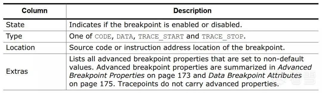 Figure 3-11 Attributes of breakpoints in Ozone
Ozone also provides many powerful features, which we will introduce one by one as we use them in the following text.
Figure 3-11 Attributes of breakpoints in Ozone
Ozone also provides many powerful features, which we will introduce one by one as we use them in the following text.
3.3.2 Debugging the Lock via SWD Interface
By reviewing the lock’s MCU chip manual, we can see that the chip provides an AES processing module, and the memory mapping of this module is shown in the following figure:
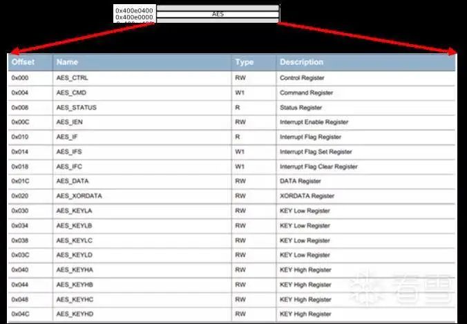 Figure 3-12 Memory mapping in EFM32
Clearly, we assume that the LuKe lock uses the chip’s AES module for encryption and decryption operations rather than implementing its own AES algorithm. Thus, we need to access the memory addresses in the range of 0x400E0000~0x400E0400. We can set appropriate read/write breakpoints and wait for the phone and lock to communicate to trigger the breakpoints.
In the breakpoint settings area, right-click and select Set Data Breakpoint. A window will pop up, as shown in the following figure:
Figure 3-12 Memory mapping in EFM32
Clearly, we assume that the LuKe lock uses the chip’s AES module for encryption and decryption operations rather than implementing its own AES algorithm. Thus, we need to access the memory addresses in the range of 0x400E0000~0x400E0400. We can set appropriate read/write breakpoints and wait for the phone and lock to communicate to trigger the breakpoints.
In the breakpoint settings area, right-click and select Set Data Breakpoint. A window will pop up, as shown in the following figure:
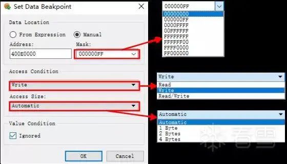 Figure 3-13 Setting data breakpoints
The settings in the figure indicate that a breakpoint will be triggered when the CPU writes data to the address 0x400E00XX.
After setting the breakpoint, click the unlock button on the phone. Since we set the data breakpoint to monitor a memory area, it will be triggered multiple times during the unlocking process. We can then see a small segment of code on the left side of the figure, while the right side shows the register data when executing at address 0xED0C.
Figure 3-13 Setting data breakpoints
The settings in the figure indicate that a breakpoint will be triggered when the CPU writes data to the address 0x400E00XX.
After setting the breakpoint, click the unlock button on the phone. Since we set the data breakpoint to monitor a memory area, it will be triggered multiple times during the unlocking process. We can then see a small segment of code on the left side of the figure, while the right side shows the register data when executing at address 0xED0C.
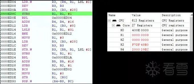 Figure 3-14 Breakpoint for writing data to be decrypted
In the figure, the address 0x400E001C (R0 + 28) is the AES_DATA register. This small segment of code is likely the AES processing function (referred to as AESFunc hereafter).
By tracing back the call stack, we can find the outer function that calls AESFunc and the starting address of the AESFunc function. We can then analyze the AESFunc function using IDA’s F5 feature, as shown in the following figure:
Figure 3-14 Breakpoint for writing data to be decrypted
In the figure, the address 0x400E001C (R0 + 28) is the AES_DATA register. This small segment of code is likely the AES processing function (referred to as AESFunc hereafter).
By tracing back the call stack, we can find the outer function that calls AESFunc and the starting address of the AESFunc function. We can then analyze the AESFunc function using IDA’s F5 feature, as shown in the following figure:
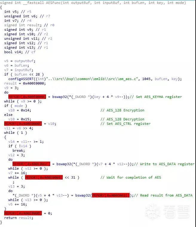 Figure 3-15 Pseudocode of the AESFunc function
Combining with the chip manual, it is easy to determine the role of each parameter in the pseudocode. In the first article of this series, we learned that the decryption key during unlocking is the BleKey, and the process of obtaining the lock’s BleKey is done by the server sending a group of data totalData to the phone app, which the app forwards directly to the lock via BLE communication without any processing. Now, let’s see how the lock processes totalData.
First, we need to look at what totalData contains, as shown in the following figure:
Figure 3-15 Pseudocode of the AESFunc function
Combining with the chip manual, it is easy to determine the role of each parameter in the pseudocode. In the first article of this series, we learned that the decryption key during unlocking is the BleKey, and the process of obtaining the lock’s BleKey is done by the server sending a group of data totalData to the phone app, which the app forwards directly to the lock via BLE communication without any processing. Now, let’s see how the lock processes totalData.
First, we need to look at what totalData contains, as shown in the following figure:
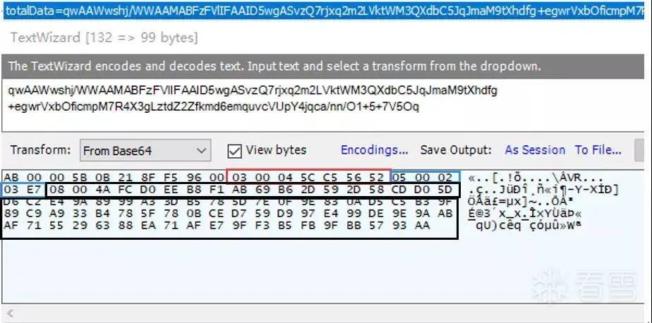 Figure 3-16 totalData field and its base64 decoded data
TotalData is a string of binary data that has been base64 encoded. The part before the red box can be considered the data header, containing message headers, packet sequence numbers, checksums, and so on. The body part after the header, i.e., the data in the red, blue, and black boxes, has the same structure, as shown in the following figure:
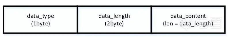 Figure 3-17 Data structure used in the payload of totalData
The data_type in the red box is 0x03, and its data_content=0x5FFFECAE, which is related to the AES root key ciphertext. The body of totalData has two other sets of data, but their specific functions will not be detailed here as it may be inappropriate to elaborate too much.
Next, we will set a breakpoint at the entrance of the AESFunc function and check the value of BleKey, as shown in the following figure:
Figure 3-17 Data structure used in the payload of totalData
The data_type in the red box is 0x03, and its data_content=0x5FFFECAE, which is related to the AES root key ciphertext. The body of totalData has two other sets of data, but their specific functions will not be detailed here as it may be inappropriate to elaborate too much.
Next, we will set a breakpoint at the entrance of the AESFunc function and check the value of BleKey, as shown in the following figure:
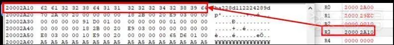 Figure 3-18 BleKey in memory
From Figures 3-16 and 3-18, we cannot see the connection between BleKey and totalData. It is likely that there is some decryption or decoding process between totalData and BleKey. We need to continue searching for the lock’s processing of totalData.
By maintaining the breakpoint in the AESFunc function during debugging, we find that totalData is also decrypted through the AESFunc function. At this point, by tracing back the call stack, we can find the critical code shown in the following figure.
Figure 3-18 BleKey in memory
From Figures 3-16 and 3-18, we cannot see the connection between BleKey and totalData. It is likely that there is some decryption or decoding process between totalData and BleKey. We need to continue searching for the lock’s processing of totalData.
By maintaining the breakpoint in the AESFunc function during debugging, we find that totalData is also decrypted through the AESFunc function. At this point, by tracing back the call stack, we can find the critical code shown in the following figure.
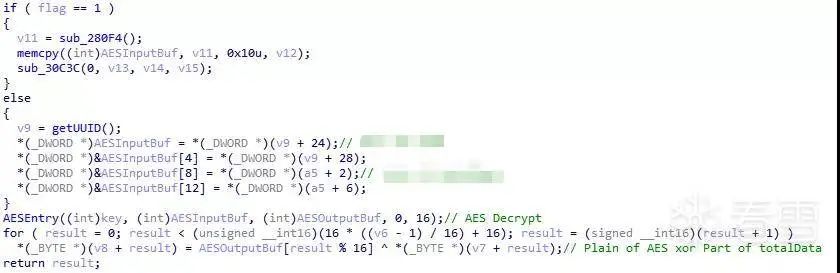 Figure 3-19 Processing of totalData
In the figure, the AESEntry function is a wrapper for the AESFunc. This part is the core code for generating BleKey from totalData, and the process can be organized in the following figure.
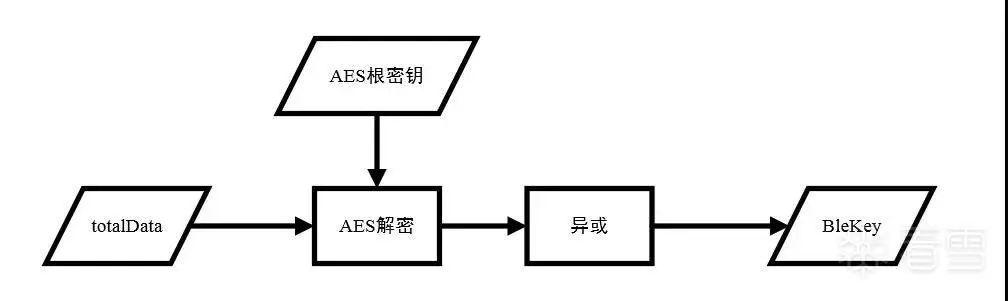 Figure 3-20 Flowchart for obtaining BleKey
In this process, if there is no root key, it is impossible to decrypt BleKey. Through debugging, we can find that the root key is stored at the Flash address 0x7E09C.
Analysis of Bootloader and FreeRTOS
In Chapter 3, we directly located the key code using the SWD debugger. This analysis method is certainly good, but it skips many valuable insights. In Chapter 4, we will take a step back and analyze this device from another perspective, starting from the first line of code after powering on the device, gradually understanding the entire firmware content.
Figure 3-20 Flowchart for obtaining BleKey
In this process, if there is no root key, it is impossible to decrypt BleKey. Through debugging, we can find that the root key is stored at the Flash address 0x7E09C.
Analysis of Bootloader and FreeRTOS
In Chapter 3, we directly located the key code using the SWD debugger. This analysis method is certainly good, but it skips many valuable insights. In Chapter 4, we will take a step back and analyze this device from another perspective, starting from the first line of code after powering on the device, gradually understanding the entire firmware content.
4.1 Bootloader Analysis
The bootloader is a piece of code that runs first after the device is powered on. It performs necessary initialization operations and guides the loading of the operating system. When we obtained the device firmware and successfully loaded it into IDA, we found that the parsed content was only a small part of the complete firmware, while much of the firmware content remained unparsed. The small part that was parsed is actually the bootloader code of the device.
To assist us in analyzing this Yunding LuKe smart lock, we can attempt to connect the device’s serial port. The serial port is located right next to the SWD interface, which can be referenced in Figure 3-1 of the second article in the Yunding LuKe smart lock series. At this point, powering on the device allows us to see string outputs from the serial port, as shown in the following figure:
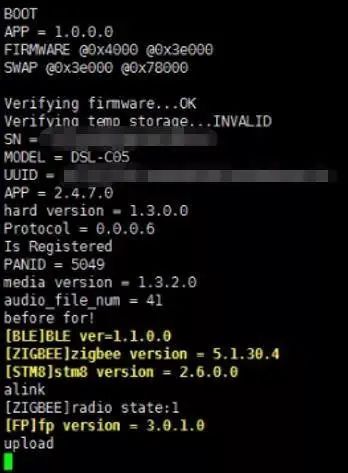
Figure 4-1 Serial output during startup
In the figure, the first few strings can be directly searched for references in IDA, while the remaining strings have not been found in the reference addresses, as shown in the following figure:
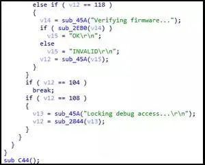 Figure 4-2 Referenced strings
 Figure 4-3 Unreferenced strings
The reason for the phenomenon in the above figure is that IDA only parsed the bootloader code. The strings in the above figure are outputs from the bootloader, while the remaining strings are outputs from the main program, which IDA failed to parse, resulting in these strings not being referenced in the code. In the figure, the program ultimately enters the sub_C44 function, as shown in the following figure:
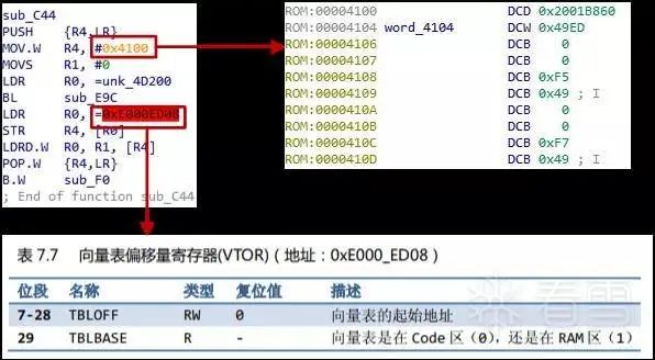 Figure 4-4 sub_C44 function
The function in the figure has a simple function: it stores 0x4100 into the vector table offset register (address 0xE000ED08), which sets the data at address 0x4100 as the new interrupt vector table. It then calls the sub_F0 function.
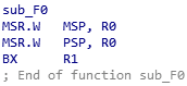 Figure 4-5 sub_F0 function
Combining Figures 4-3 and 4-4, the bootloader will ultimately set 0x2001B860 (the value at address 0x4100) as the new stack pointer and jump to 0x49ED (the value at address 0x4104). After this, the bootloader hands over control of the MCU to the main program.
In summary, after powering on the device, the bootloader will first execute, search and verify the firmware in Flash, and upon successful verification, set a new interrupt vector table and jump to the entry address of the main program.
Figure 4-5 sub_F0 function
Combining Figures 4-3 and 4-4, the bootloader will ultimately set 0x2001B860 (the value at address 0x4100) as the new stack pointer and jump to 0x49ED (the value at address 0x4104). After this, the bootloader hands over control of the MCU to the main program.
In summary, after powering on the device, the bootloader will first execute, search and verify the firmware in Flash, and upon successful verification, set a new interrupt vector table and jump to the entry address of the main program.
4.2 FreeRTOS Analysis
Through the strings in the firmware, we can infer that the device uses the FreeRTOS operating system, which is a very common open-source real-time operating system. Its official homepage is: https://www.freertos.org.
In devices using FreeRTOS, the firmware main program is a binary file that intermingles FreeRTOS kernel code and application logic code. Therefore, we need to find a way to distinguish between the two; otherwise, we may encounter errors similar to analyzing MFC42.
The FreeRTOS operating system provides task management capabilities, and the logical functions of the device are implemented by one or more tasks. Thus, the application logic code must be in the implementation code of these tasks. The API for creating tasks in the FreeRTOS system is shown in the following figure:
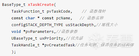 Figure 4-6 FreeRTOS task creation API
In the figure, the first parameter of the function is the function pointer corresponding to the task, and the second parameter is the name of the task. As long as we find the calling points of this API, we can locate the task functions through its first parameter.
Since FreeRTOS is an open-source operating system, we can compile the source code to generate a program with a symbol table, and then use the bindiff plugin of IDA to compare and identify the FreeRTOS operating system APIs in the firmware.
The bindiff plugin is an IDA plugin used to compare similar functions in two idb (IDA database) files, commonly used in vulnerability patch analysis. Its official website is https://www.zynamics.com/bindiff.html. According to the installation instructions on the official website, download the appropriate version of the bindiff installation program, and complete the installation to use it.
To improve the accuracy of the bindiff plugin comparison, we should try to select a version of FreeRTOS that is similar to that used by Yunding LuKe, and the compilation environment and configuration should also be as close to that of the Yunding LuKe smart lock as possible. Interestingly, during our search for available source code, we unexpectedly found a code repository on GitHub that is extremely similar to the firmware we are reverse engineering.
The link is https://github.com/RunningChild/efm32_freertos_app. After discovering that the owner of this repository is a staff member from Yunding LuKe, we found that this code is the remaining FreeRTOS framework after all the key application logic code was deleted.
After successfully compiling the project, we can use the bindiff plugin for comparison. The specific compilation method and process will be organized and introduced in future articles, so we will not elaborate too much in this article. Some comparison results are shown in the following figure:
 Figure 4-7 Partial results of bdiff
In the figure, the xTaskGenericCreate function in our compiled firmware is very similar to the sub_34A50 function in the original firmware, indicating that sub_34A50 is the API interface for creating tasks in FreeRTOS. We will then look for references to the sub_34A50 function in IDA, and one of the references is shown in the following figure:
 Figure 4-8 Call to sub_34A50
In the figure, the parameters of the sub_34A50 function match those of the xTaskCreate in Figure 4-6. We can also determine that the function at address 0x1B0A9 is responsible for receiving and processing BLE messages. We will set a breakpoint at address 0x1B0A8 and start debugging. When the unlock button is clicked in the phone app, the breakpoint will be triggered, allowing us to continue analyzing from this clue.
Thus, we can confirm that the sub_34A50 function is the API used by the firmware to create tasks. Next, we only need to write a simple IDA Python script to list all the tasks in the firmware, and IDA will create functions at the addresses of these tasks. The script is shown in the figure:
Figure 4-8 Call to sub_34A50
In the figure, the parameters of the sub_34A50 function match those of the xTaskCreate in Figure 4-6. We can also determine that the function at address 0x1B0A9 is responsible for receiving and processing BLE messages. We will set a breakpoint at address 0x1B0A8 and start debugging. When the unlock button is clicked in the phone app, the breakpoint will be triggered, allowing us to continue analyzing from this clue.
Thus, we can confirm that the sub_34A50 function is the API used by the firmware to create tasks. Next, we only need to write a simple IDA Python script to list all the tasks in the firmware, and IDA will create functions at the addresses of these tasks. The script is shown in the figure:
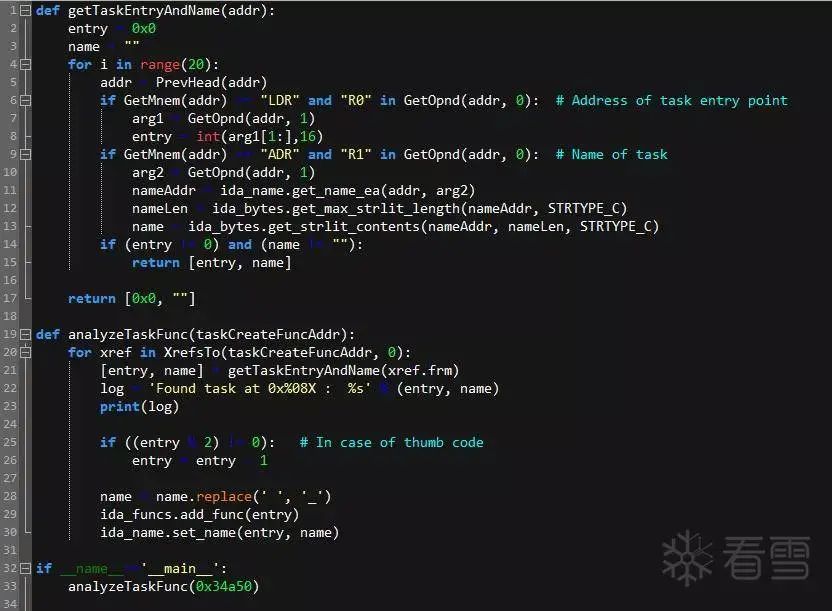 Figure 4-9 Script for parsing task entry functions in IDA
The results of running the script are as follows:
Figure 4-9 Script for parsing task entry functions in IDA
The results of running the script are as follows:
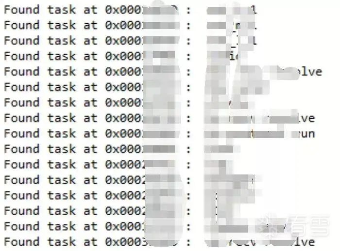 Figure 4-10 Output of the script results
Note that the script’s functionality relies on cross-references to the sub_34A50 function, which may miss some tasks due to some references not being recognized by IDA. At this point, we can freely analyze the functional points of interest in the Yunding LuKe smart lock.
Thus, the analysis of the Yunding LuKe smart lock comes to an end. In this article, we explored the AES encryption protection in the communication data of the lock’s Bluetooth functionality by reverse engineering the mobile APK.
We then shared how to use the SWD interface to extract firmware and further analyze the process of obtaining BleKey by debugging the lock’s firmware. Finally, we focused on analyzing the bootloader code and the FreeRTOS operating system after the device starts up.
As an open-source real-time operating system, FreeRTOS indeed has a considerable user base. Although analyzing it may be a bit more complicated than programs of embedded Linux operating systems, it is still recommended that readers have a simple understanding of it.
I hope this article can bring some gains to readers. If you have any discussions or inquiries, feel free to contact us via WeChat: PwnMonkey. In future articles, we will continue to share other research cases, so stay tuned.
Figure 4-10 Output of the script results
Note that the script’s functionality relies on cross-references to the sub_34A50 function, which may miss some tasks due to some references not being recognized by IDA. At this point, we can freely analyze the functional points of interest in the Yunding LuKe smart lock.
Thus, the analysis of the Yunding LuKe smart lock comes to an end. In this article, we explored the AES encryption protection in the communication data of the lock’s Bluetooth functionality by reverse engineering the mobile APK.
We then shared how to use the SWD interface to extract firmware and further analyze the process of obtaining BleKey by debugging the lock’s firmware. Finally, we focused on analyzing the bootloader code and the FreeRTOS operating system after the device starts up.
As an open-source real-time operating system, FreeRTOS indeed has a considerable user base. Although analyzing it may be a bit more complicated than programs of embedded Linux operating systems, it is still recommended that readers have a simple understanding of it.
I hope this article can bring some gains to readers. If you have any discussions or inquiries, feel free to contact us via WeChat: PwnMonkey. In future articles, we will continue to share other research cases, so stay tuned.
Kanxue ID: Hu Yimi
https://bbs.pediy.com/user-home-613694.htm
*This article is original by Kanxue Forum Hu Yimi, please indicate the source from Kanxue Community when reprinting
# Previous Recommendations
1. Windows Driver Programming: WFP/TDI
2. A MEMZ Sample Analysis
3. Exploring Dex
4. Windows Driver Programming: NetFilter SDK
5. Analysis of GlobeImposter Family Virus Samples
6. CVE-2010-2553 Heap Overflow Vulnerability Analysis
Public Account ID: ikanxue
Official Weibo: Kanxue Security