SoC (System on Chip) refers to a system-level chip that integrates key components such asCPU, memory controllers, peripheral interfaces, andAI acceleration units. With advantages of high performance, low power consumption, and miniaturization,SoC is widely used in mobile phones, tablets, and smart home devices.
This article takes theMT8519 SoC produced by MediaTek as an example to analyze its internal architecture and the functions of various modules.
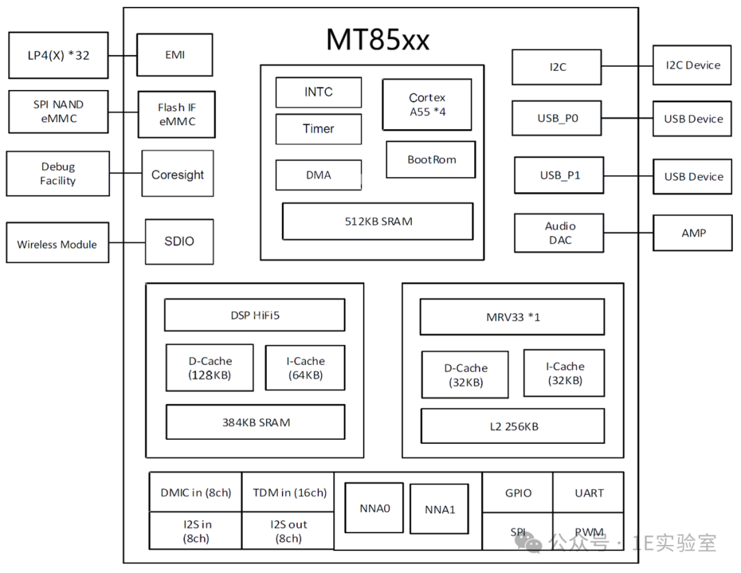
▲ Block diagram of MT85xx SoC
1. CPU System
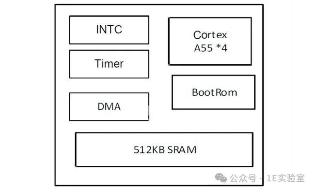
▲ CPU System
1.1 Cortex-A55 CPU Core
Cortex-A55 is a 64-bit processor core designed by ARM based on the ARMv8.2-A architecture, used in consumer electronics. Cortex is the brand name, while A55 is the model.
The advantages of using a quad-core CPU include: four cores working in parallel, the ability to shut down or reduce the frequency of some cores to lower power consumption during low load, and all cores running to improve overall energy efficiency during high load.
1.2 Other Modules
Boot ROM (Boot Read Only Memory) stores firmware internally and is responsible for power-on initialization, secure boot verification, and loading subsequent boot programs.
INTC (Interrupt Controller) manages interrupt requests from peripherals and distributes them to the CPU cores based on priority, ensuring real-time response.
TIMER (Timer) is a hardware module used for precise timing and event triggering, which works by counting fixed-period clock pulses and triggering interrupts when the count reaches a preset value. The timer can also be used for generating PWM signals.
DMA (Direct Memory Access Controller) is a hardware module that can complete data transfer between memory and peripherals without CPU intervention, reducing the CPU’s burden and improving data throughput, suitable for network communication and audio-video processing scenarios.
SRAM (Static Random Access Memory) uses bistable latches (six-transistor structure) to store data, characterized by the ability to maintain state without refresh, data loss on power down, faster read/write speeds than DRAM, low power consumption, and good stability. The 512KB SRAM here serves as the shared cache for the quad-core CPU cluster, belonging to L3 Cache, used to compensate for the limitations of the CPU cache capacity.
2. DSP System
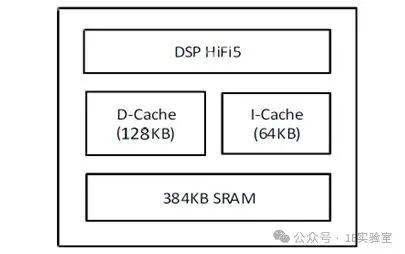
▲ DSP System
2.1 HiFi5 DSP
HiFi5 is a high-performance DSP (Digital Signal Processor) core designed by Cadence, specifically optimized for far-field audio processing and AI voice recognition scenarios, supporting 5 paths of VLIW (Very Long Instruction Word) and SIMD (Single Instruction Multiple Data) parallel computing. Compared to the previous generation HiFi4 DSP, its audio processing performance has doubled, and neural network computing power has increased fourfold.
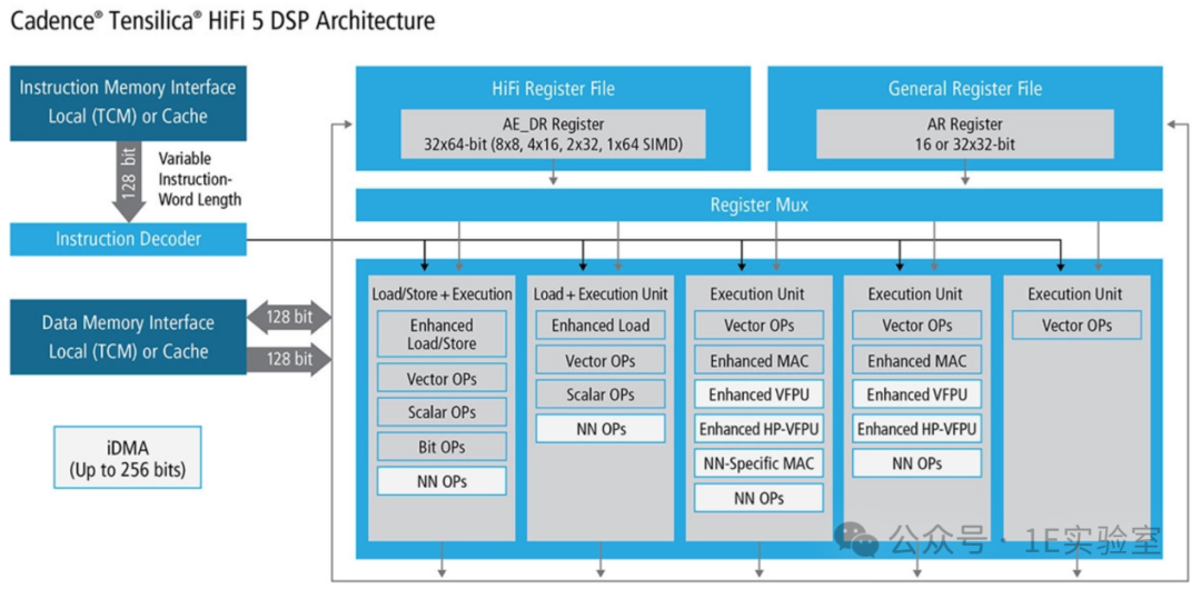
▲ HiFi DSP Architecture
HiFi5 DSP can run complex voice algorithms, enabling features such as adaptive ANC (Active Noise Cancellation), AI noise reduction, 3D sound enhancement, spatial audio partitioning, and far-field voice wake-up, applicable in headphones, automotive, and smart home scenarios.
2.2 D-Cache and I-Cache
Data Cache and Instruction Cache are both level 1 caches of the DSP, where the data cache stores frequently accessed data copies, and the instruction cache stores frequently executed instruction copies. These two caches are designed separately, forming a Harvard architecture to avoid conflicts between instruction and data access.
2.3 SRAM
The system has designed low-latency SRAM specifically for the HiFi5 DSP, primarily to cache intermediate results in audio processing (such as filter coefficients, FFT computation data) or weight parameters for neural network inference, avoiding high latency from frequent access to external main memory (such as DRAM); secondly, in real-time audio processing (such as noise reduction, voice wake-up), the low latency of SRAM ensures the timing of algorithm execution; finally, using SRAM also has the advantage of low power consumption.
3. RV33 Processor Subsystem
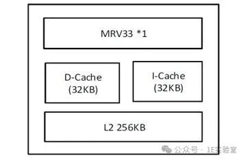
▲ RV33 Processor Subsystem
The RV33 subsystem is a relatively independent processor system with its own power supply and SRAM. This special design allows the RV33 to run specific functions, such as voice wake-up, even when the SoC is in sleep mode. The RV33 subsystem can also access DRAM, system SRAM, and other hardware resources via the infra bus.
The RV33 subsystem includes a small RV33 processor, 32KB data cache, 32KB instruction cache, and 256KB L2 cache (SRAM). The RV33 is a 32-bit processor core based on the RISC-V instruction set architecture.
4. Audio Interfaces, NNA and Common Interfaces
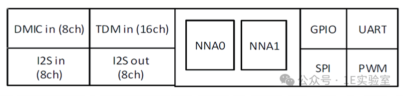
▲ Audio Interfaces, NNA and Common Interfaces
4.1 Audio Interfaces
The MT85xx SoC supports various audio interfaces, including 8 channels of DMIC (Digital Microphone) input, 16 channels of TDM (Time Division Multiplexing Audio) input, 8 channels of I2S (Inter-IC Sound) input, and 8 channels of I2S output.
Among them, the 8 channels of DMIC are implemented by multiplexing four DMIC data interfaces: two microphones share the same data line but sample data using the rising and falling edges of the clock respectively.16 channels of TDM correspond to only one TDM data interface in hardware, also using time division multiplexing.8 channels of I2S correspond to four I2S data interfaces, multiplexing left and right channels through I2S_LRCK.
4.2 NNA
NNA (Neural Network Accelerator) is a processor specifically designed for neural network computations, mainly used for efficiently executing inference tasks in deep learning.The hardware architecture of the NNA includes computing units, storage systems, control units, and data buses.
4.3 Common Interfaces
The SoC features common GPIO (General Purpose Input/Output), UART (Universal Asynchronous Receiver/Transmitter), SPI (Serial Peripheral Interface), and PWM (Pulse Width Modulation) interfaces.
5. Other Interfaces
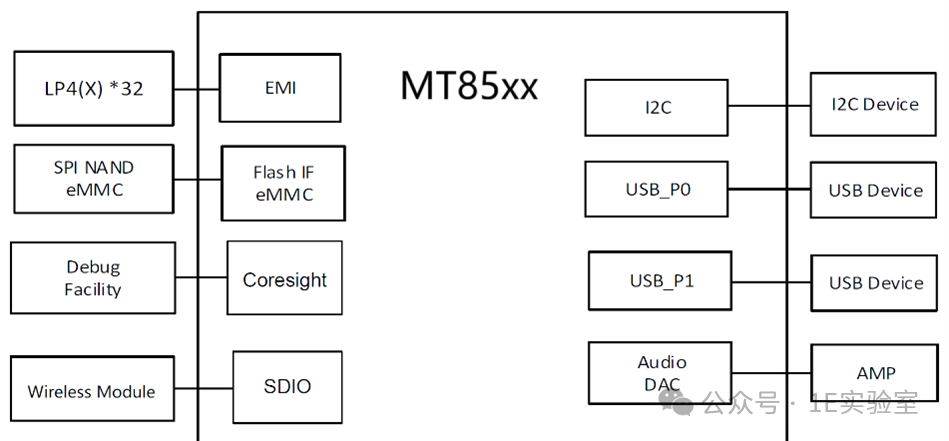
▲ Other Interfaces
EMI (External Memory Interface) is the interface that connects the SoC to LPDDR4 memory chips. This abbreviation is also shared with EMI (Electromagnetic Interference)).
The chip has interfaces for external SPI Nand Flash and eMMC (embedded Multi-Media Card) storage.
CoreSight is a debugging system based on the ARM architecture.
SDIO (Secure Digital Input/Output) is an external bus interface used to connect various peripherals, such as WiFi/Bluetooth modules.
I2C (Inter-Integrated Circuit) is a common two-wire serial interface for connecting external hardware.
USB (Universal Serial Bus) is a common serial interconnection interface.
Finally, the SoC also integrates a DAC (Digital Analog Converter), which outputs analog audio signals to an AMP (Amplifier), used to drive speakers.
Conclusion
This article outlines the key hardware modules and functional characteristics of the MT85xx SoC chip, covering the three core components: Cortex-A55 CPU, HiFi5 DSP, and RV33 processor. This chip achieves an optimized balance between performance and energy efficiency through a heterogeneous computing architecture and highly integrated design, commonly used in smart speaker devices.