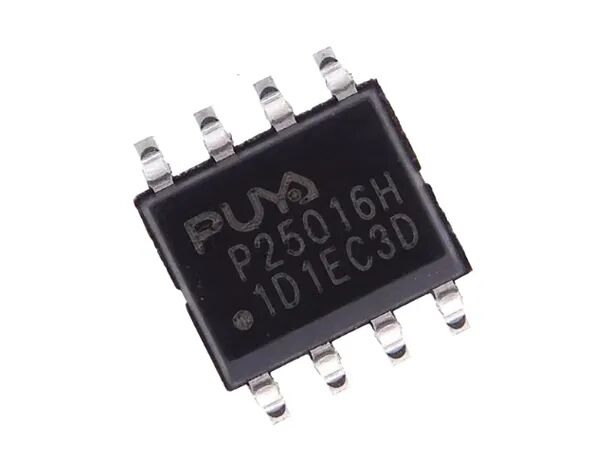
ACROVIEW, a leader in chip programming technology, recently announced the latest iteration of its programming software, unveiling a series of newly compatible chip models. In this update, the serial interface flash memory P25Q16SH-SS from PUYA Semiconductor has been supported by the chip programming device AP8000.

P25Q16SH-SS is a serial interface flash memory device designed for various high-capacity consumer applications, where program code is copied from flash memory to embedded or external RAM for execution. This device features a flexible erase architecture and page erase granularity, making it ideal for data storage without the need for additional data storage devices.
The erase block size of P25Q16SH-SS is optimized to meet the demands of today’s code and data storage applications. By optimizing the erase block size, storage space can be utilized more efficiently. Since certain code modules and data storage segments must reside in their own erase areas, this significantly reduces waste and unused storage space compared to flash memory devices that use large sectors and blocks for erasure. This increased storage space efficiency allows for the addition of extra code routines and data storage segments while maintaining the same overall device density.
P25Q16SH-SS also includes three additional 1024-byte security registers with one-time programmable (OTP) locking capabilities, which can be used for unique device serialization, system-level electronic serial number (ESN) storage, key storage, and more.
P25Q16SH-SS is designed for various systems and supports read, program, and erase operations within a wide power supply voltage range of 2.3V to 3.6V. Programming and erasing operations do not require a separate voltage.
Features
• Single power supply voltage range: 2.3V to 3.60V
• Industrial temperature range: -40°C to 85°C
• Compatible with Serial Peripheral Interface (SPI): Mode 0 and Mode 3
• Supports Single SPI, Dual SPI, Quad SPI, QPI (Quad Peripheral Interface), and DTR (Double Transfer Rate Read)
– Standard SPI: SCLK (Clock), CS# (Chip Select), SI (Data Input), SO (Data Output), WP# (Write Protect), HOLD# (Hold)
– Dual SPI: SCLK, CS#, IO0, IO1, WP#, HOLD#
– Quad SPI: SCLK, CS#, IO0, IO1, IO2, IO3
– QPI: SCLK, CS#, IO0, IO1, IO2, IO3
– DTR: Double Transfer Rate Read
• Flexible code and data storage architecture
– Uniform 256-byte page programming
– Uniform 256-byte page erase
– Uniform 4K-byte sector erase
– Uniform 32K/64K-byte block erase
– Full chip erase
• Hardware control protection for locking sectors via WP pin
• One-time programmable (OTP) security registers
– 3*1024-byte security registers with OTP locking
• Each device has a unique 128-bit ID
• Fast programming and erase speeds
– Single/Dual/Quad page programming time: 1.5 milliseconds
– Page erase time: 16 milliseconds
– 4K-byte sector erase time: 16 milliseconds
– 32K/64K-byte block erase time: 16 milliseconds
• JEDEC standard manufacturer and device ID reading methods
• Ultra-low power consumption
– Deep power-down current: 0.5 microamps
– Standby current: 10.0 microamps
– Active read current at 85MHz: 5.0 milliamps
– Active programming or erase current: 3.0 milliamps
• High reliability
– 100,000 programming/erase cycles
– 20 years data retention time
• Environmentally friendly packaging options compliant with industry standards
– 8-pin SOP (150 mil/208 mil)
– 8-pad USON (3x2x0.55mm, 3x4x0.55mm, 3x2x0.45mm)
– 8-pad WSON (6x5x0.75mm)
– 8-pin TSSOP
– KGD (Known Good Die) for SiP
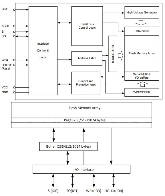
Internal Block Diagram
The AP8000 universal programmer developed by ACROVIEW supports both online/offline versions with one-to-one and one-to-eight configurations, as well as dedicated programming solutions for eMMC and UFS, fully covering the bare chip (offline) and on-board programming needs for all chip models in the PUYA series. The AP8000 consists of three core components: the host, the motherboard, and the adapter. As a universal programming platform in the industry, the AP8000 not only supports programming for all types of programmable chips available in the market but also serves as the core programming platform for ACROVIEW’s automated IPS5800S batch secure programming, efficiently executing large-scale programming tasks.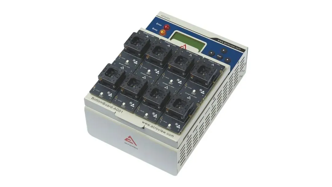
The host supports both USB and NET connections, enabling networking of multiple programmers to synchronize control for programming operations. The built-in safety protection circuit can instantly detect abnormal situations such as reversed chip placement or short circuits, immediately cutting off power to ensure the safety of both the chip and the programmer. The host integrates a high-speed FPGA, significantly enhancing data transmission and processing speeds. The back of the host features an SD card slot, allowing users to save project files generated by PC software to the root directory of the SD card and insert it into the slot. By using the button on the programmer, users can select, load, and execute programming instructions without relying on a PC, which not only reduces the hardware configuration costs of the PC but also facilitates the rapid construction of the working environment.
The AP8000’s combination design of the motherboard and adapter greatly enhances the host’s expansion capabilities, currently supporting products from all major semiconductor manufacturers, including SINO WEALTH, semidrive, winbond, holychip, ESMT, and others. The types of devices supported include NAND, NOR, MCU, CPLD, FPGA, EMMC, etc., and it is compatible with various file formats such as Intel Hex, Motorola S, Binary, POF, etc.
Company Introduction
About PUYA Semiconductor:PUYA Semiconductor is a supplier of low-power SPI NOR Flash memory chips and high-reliability IIC EEPROM memory chips. As an innovator in the semiconductor industry, PUYA collaborates with leading domestic wafer fabs, integrating advanced design and process advantages to develop low-power, high-reliability NOR-type serial Flash memory products in the 28nm to 55nm range, applicable to traditional consumer and industrial markets as well as emerging application markets, offering highly competitive bare chip sizes and high-performance advantages, making it an excellent choice for MCP and MCU solution providers. PUYA’s 130nm non-volatile IIC EEPROM memory features industry-leading 4 million erase/write cycles, 6KV electrostatic protection, extremely low operating current, and static power consumption, widely used in smart grids, automotive front-end, industrial control, and emerging IoT fields.
About ACROVIEW:ACROVIEW is a global leader in semiconductor chip programming solutions, committed to changing the world through technology and driving the future with intelligence, continuously creating value for customers. ACROVIEW’s AP8000 universal programmer platform and the latest IPS5800S programming automation solution provide one-stop solutions for customers in the semiconductor and electronics manufacturing fields, having served leading global clients including Huawei, BYD, Foxconn, and others.
Scan to follow us

ACROVIEW Service Account

ACROVIEW Subscription Account