2.4
Boot Modes of Renesas RA Chips
2.4.1
Introduction to Boot Modes of Renesas RA Chips
When powered on or reset via the chip reset pin, the RA chip enters different operational modes based on the level of the MD pin: “Single-chip Mode” or “Boot Mode”.
-
“Single-chip Mode” is the normal operating mode where the user’s code runs;
-
“Boot Mode” is the factory code mode, where the code running is a built-in code that cannot be modified, provided by Renesas at the time of manufacture.
The Boot modes of RA6M5 and RA4M2 support both SCI boot and USB boot, as shown in the figure below:
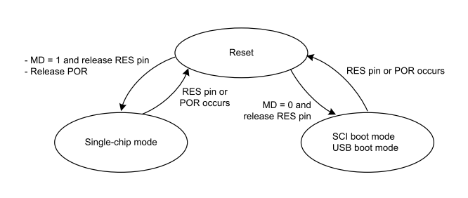
As seen in the figure above, the Boot mode can be controlled by the MD pin and the chip reset pin.
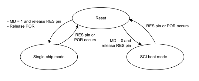
RA2L1, lacking USB functionality, only supports SCI boot in its Boot mode, as shown in the figure below:
2.4.2
Setting Boot Mode on the Wildfire Qiming Development Board
The specific steps to manually set the Wildfire Qiming 6M5 and Qiming 4M2 development boards to enter Boot mode are as follows:
-
First, connect the wiring.
-
For USB Boot, connect via a Type C USB cable to the USB Device interface on the development board;
-
For SCI Boot, connect via USB to serial to the two pins on the JTAG debug interface: P109 (TDO/TXD9) and P110 (TDI/RXD9).
-
Next, use a jumper cap to change the MD pin from high level (3V3) to low level (GND), then manually press the reset button on the development board to enter Boot mode.
Note:The Wildfire Qiming 2L1 development board does not support entering Boot mode.
-
Due to the two pins of the RA2L1 chip on the Qiming 2L1 development board: P109 (TDO/TXD9) and P110 (TDI/RXD9) being reused for CAN functionality connected to the CAN transceiver chip, the Wildfire Qiming 2L1 development board does not support entering Boot mode.
In fact, when using JLink, the e2 studio or Renesas Flash Programmer (RFP) software will automatically switch to Boot mode via JLink when needed. This method does not require us to manually switch the MD pin level to enter Boot mode; simply short the MD pin to the TCK pin on the JTAG interface:
-
That is, remove the jumper cap from the J17 header on the Qiming 6M5/Qiming 4M2 development board, and then insert the jumper cap onto J23 next to the JTAG interface.
Annotation
Note that the J-Link here requires J-Link V10 or later hardware versions; earlier versions and JLink EDU mini do not support this function.
2.5
Using Renesas Flash Programmer Software
Changing the Chip DLM State
-
First, manually set the chip to enter Boot mode as described above.
-
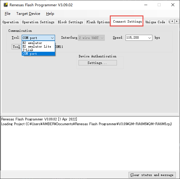
Then open the Renesas Flash Programmer (RFP) software, create a new project, and set the connection method.
-
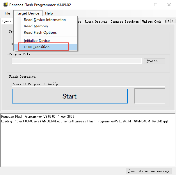
Finally, switch the DLM state or change other configuration parameters.
Setting Communication Connection Method:
Converting Chip DLM State:


Need Technical Support?
If you have any questions while using Renesas MCU/MPU products, you can scan the QR code below or copy the URL into your browser to access the Renesas Technical Forum for answers or online technical support.

https://community-ja.renesas.com/zh/forums-groups/mcu-mpu/
To be continued
Recommended Reading

Introduction to ARM Microcontrollers and Overview of Renesas RA Series MCUs – Renesas RA Series FSP Library Development Practical Guide Series (03)
Naming Method and Selection of Renesas RA Series MCUs – Renesas RA Series FSP Library Development Practical Guide Series (04)

Introduction to TrustZone and Its Uses with Device Lifecycle Management (DLM) – Renesas RA Series FSP Library Development Practical Guide Series (05)