Continuing with the circuit design around the TJ375N1156X, today we will introduce the eMMC interface and the SD card interface.
1. eMMC Interface
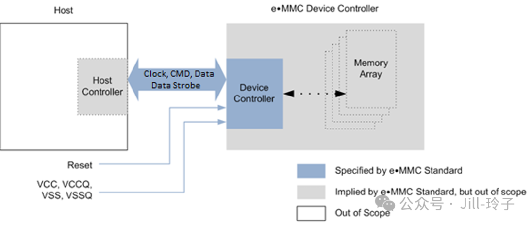
eMMC: Embedded Multi Media Card, as shown in the diagram below, the internal structure of eMMC packages NAND Flash and the eMMC controller together, providing a standard interface that allows eMMC to automatically adjust its operating mode with the host, making it easy for the system to be compatible with different NAND Flash types.
The following diagram illustrates the overall architecture of eMMC:
 The standard eMMC interface includes the following signals:
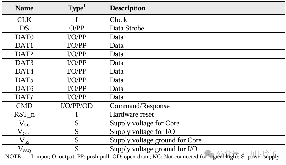 The four types of signal functions for eMMC are described as follows:Clock Signal: CLK: The read/write clock provided by the host to the eMMC.Control Signals: 1): DS: The DS signal is sent from eMMC to the host, with a clock frequency the same as the CLK signal, used to synchronize the data output from the device side, utilized in HS400 mode to achieve data synchronization at the host end.2): CMD: Command interaction signal, used to transmit control commands or respond to the host (sending the host’s command and the device’s response), a bidirectional signal, operating in open-drain and push-pull modes. Communication between the host and eMMC is initiated by the host with a command, and the device responds differently based on the command.3): RST_n: Reset signal.Data Signals: DAT[7:0]: Bidirectional data. The bidirectional data bus of eMMC is used for data communication between the host and the device. The DAT signal can only support unidirectional transmission at any given time, controlled by either the eMMC or the eMMC HOST. By default, when the user powers on or resets, data can only be transmitted using the DAT0 line. Additionally, users can configure the number of DAT lines they wish to use, choosing either 4 or 8 lines. When 4 lines are selected, the eMMC device will disconnect the internal pull-up of DAT1-3, requiring external pull-up by the user. When 8 lines are selected, similarly, the internal pull-up of DAT1-7 will be disconnected, requiring external pull-up by the user.Power Signals: VCC: Core power supply for eMMC. VCCQ: IO power supply. [Note: The selection of eMMC devices must match the voltage of the connected BANK. If connecting to HVIO, choose eMMC devices that support 3V for VCCQ; if connecting to HSIO, choose eMMC devices that support 1.8V for VCCQ.]eMMC Interface Operating Rates:The table below summarizes the different operating rate modes of the eMMC interface:
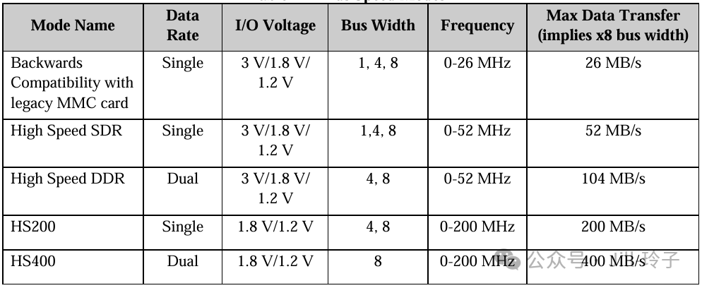 Among these, the most commonly used are HS200 and HS400 modes.HS200 Rate Mode:The HS200 mode offers the following features:* SDR Data sampling method (single edge sampling) * CLK frequency up to 200 MHz Data rate – up to 200 MB/s * 4 or 8-bits bus width supported * Single-ended signaling with 4 Drive Strengths * Signaling levels of 1.8 V and 1.2 V * Tuning concept for Read Operations
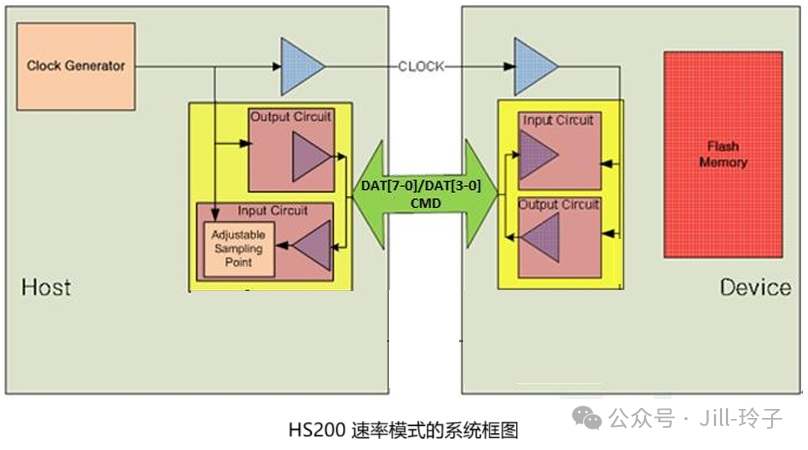
HS400 Bus Speed Mode:
HS400 mode has the following features:
* DDR Data sampling method (double edge sampling)
* CLK frequency up to 200 MHz, Data rate is up to 400 MB/s
* Only 8-bit bus width supported
* Signaling levels of 1.8 V and 1.2 V
* Support up to 5 Drive Strengths
* Data strobe signal is toggled only for Data out, CRC response, and CMD Response
HS400 mode system framework diagram: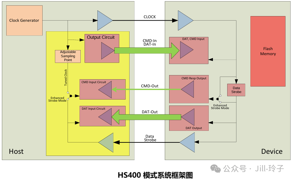
eMMC Internal Partitioning:
Having understood the interface signals and operating modes of eMMC, we can also get a general idea of the internal partitioning of eMMC, which helps us better understand the functionality of the eMMC interface.
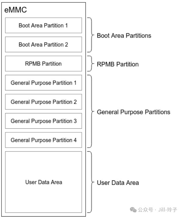
Function descriptions of each partition:
BOOT Area Partition 1 & 2
This partition is primarily designed to support system booting from eMMC. The data in this partition can be read out through a simple protocol after powering on the eMMC. Additionally, most SOCs can configure the ROM code to load the contents of the eMMC BOOT partition into the internal SRAM of the SOC upon power-up via GPIO or FUSE configuration.
RPMB Partition
RPMB stands for Replay Protected Memory Block, which is a secure partition within eMMC. When writing data to RPMB, eMMC verifies the legality of the data, allowing only designated hosts to write. During data reading, a signature mechanism is also provided to ensure that the host reads data from within RPMB and not from forged data by an attacker.
In practical applications, RPMB is typically used to store data that requires protection against unauthorized tampering, such as public keys and serial numbers related to fingerprint payment on mobile phones. RPMB can authenticate write operations, but reading does not require authentication, allowing anyone to perform read operations. Therefore, data stored in RPMB is usually encrypted before storage.
General Purpose Partition 1~4
This area is mainly used for storing system or user data. The General Purpose Partition typically does not exist at the factory and must be actively configured to be present.
User Data Area
This area is primarily used for storing system and user data. The User Data Area is usually subject to repartitioning.
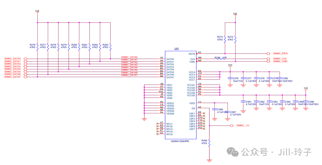
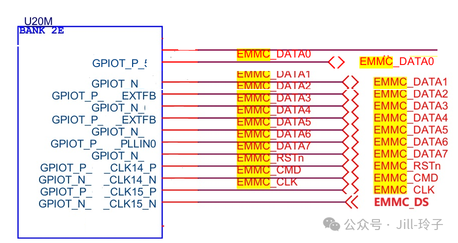
eMMC Hardware Interface Design
According to the eMMC standard, the hardware circuit connection for the eMMC interface is referenced in the diagram below:
[Note: The eMMC device selected in the diagram has a VCCQ of 1.8V, and the eMMC signals are connected to the HSIO of the TJ375N1156X. Specific pins need to be allocated by the user.]
 The PCB design for the eMMC interface: Since the eMMC data lines belong to a high-speed parallel bus, the PCB routing is recommended to: 1): Route signal lines on inner layers, ensuring good reference ground planes for the signal lines. 2): Ensure equal length for data lines. 3): Maintain a distance of 5 times the line width between the CLK signal and Data signals. 2. SD Card Interface: The SD card is a portable storage card implemented with flash memory. The most commonly used are SD cards and SDHC cards (High Capacity SD Memory Card), both of which comply with the SD 2.0 protocol.SDIO BusSDIO is the communication bus between the host (reader) and the card (SD card), consisting of 6 signals (as shown in the table below), with a voltage standard of 3.3V (0V for logic 0, 3.3V for logic 1).
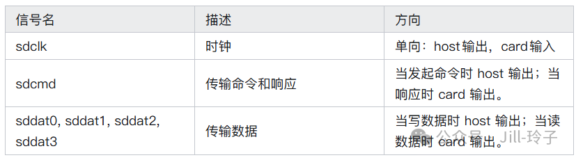 Common SD cards are divided into standard size SD cards and micro-SD cards, which differ only in physical dimensions but have no functional differences. Here, we choose the micro-SD card. The following diagram illustrates the differences between standard size SD cards and micro-SD cards:
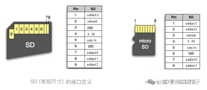 Reference Circuit Diagram for SD CardThe following diagram provides the reference circuit diagram for the SD card interface: Note: The operating voltage for the SD card is 3.3V, so it needs to be connected to the 3.3V BANK of the TJ375N1156X. Additionally, the card presence detection signal has no requirements for the connected BANK, but its pull-up level must match the voltage of the connected BANK.
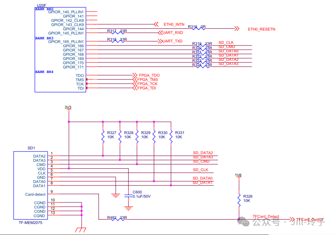 As for the specific signal timing and related command formats, please refer to the relevant standards; here we will only introduce the hardware connections. 【To be continued】