A Comprehensive Guide to CPU Architecture

Source: Semiconductor Industry Observation

The CPU, often referred to as the brain of the computer, consists of several parts, including those that receive information, store information, process information, and assist in outputting information. These parts work together to process information.
In today’s article, we will introduce the key elements that make up the CPU and how they work together to provide power to the computer.
A Comprehensive Guide to CPU Architecture

CPU Blueprint: ISA

When analyzing any CPU, the first thing you encounter is the Instruction Set Architecture (ISA). This is a graphical blueprint of how the CPU operates and how all internal systems interact. Just as there are many breeds of dogs within the same species, many different types of ISA can be built on a CPU. The two most common types are x86 (found in desktops and laptops) and ARM (found in embedded and mobile devices).
There are also some niche applications like MIPS, RISC-V, and PowerPC. The ISA specifies which instructions the CPU can process, how it interacts with memory and cache, and how work is divided across multiple processing stages, etc.
To cover the main parts of the CPU, we will follow the path taken by an instruction when it is executed. Different types of instructions may follow different paths and use different parts of the CPU, but here we will generalize to cover the largest parts. We will start with the most basic design of a single-core processor and gradually increase complexity as we move toward more modern designs.

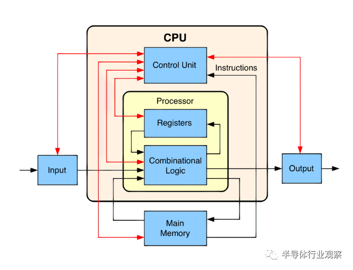
Control Unit and Data Path

The CPU can be divided into two parts: the control unit and the data path.Imagine a train. The engine is the power source of the train, but the conductor pulls the levers and controls various aspects of the engine behind the scenes. The CPU works in the same way.
The data path, as the name suggests, is the path through which data flows during processing. The data path receives input, processes it, and sends it to the correct location upon completion. The control unit tells the data path how to operate. Depending on the instruction, the data path routes signals to different components, turning different parts of the data path on and off, and monitoring the status of the CPU.
A Comprehensive Guide to CPU Architecture

Instruction Cycle – Fetch

The first thing our CPU must do is figure out what instruction to execute next and then transfer it from memory into the CPU. Instructions are generated by the compiler and are specific to the CPU’s ISA. The ISA shares the most common types of instructions, such as load, store, addition, subtraction, etc., but each specific ISA has many other special types of instructions. For each type of instruction, the control unit will know which signals to route where.
For example, when you run a .exe on Windows, the program’s code is moved into memory, telling the CPU the starting address of the first instruction. The CPU always maintains an internal register that holds the memory location of the next instruction to be executed. This is called the Program Counter (PC).
Once it knows where to start, the first step of the instruction cycle is to fetch that instruction. This moves the instruction from memory into the CPU’s instruction register, known as the fetch stage. In practice, the instruction may already be in the CPU’s cache, which we will discuss later.

Instruction Cycle – Decode

When the CPU has an instruction, it needs to figure out what type of instruction it is. This is called the decode stage. Each instruction will have a specific set of bits called the opcode that tells the CPU how to interpret it. This is similar to how different file extensions tell the computer how to interpret files. For example, .jpg and .png are both image files, but they organize data differently, so the computer needs to know the type to interpret them correctly.
Depending on the complexity of the ISA, the instruction decoding part of the CPU can become complex. An ISA like RISC-V may have only dozens of instructions, while x86 has thousands. On a typical Intel x86 CPU, the decoding process is one of the most challenging and takes up a lot of space. The most common types of instructions that the CPU decodes are memory, arithmetic, or branch instructions.

Three Main Instruction Types
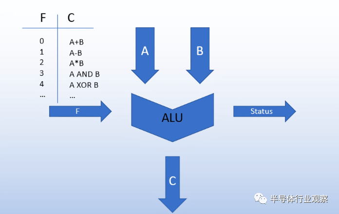
Memory instructions might look like “read value A from storage address 1234” or “write value B to storage address 5678”. Arithmetic instructions might look like “add value A to value B and store the result in value C”. Branch instructions might look like “if C is positive, execute this code; if C is negative, execute that code.” A typical program might link them together to produce something like “add the value at memory address 1234 to the value at memory address 5678 and store the result at memory address 4321, and if the result is negative, store something at address 8765.”
Before we start executing the just-decoded instruction, we need to pause for a moment to discuss registers.
The CPU has a small but very fast memory called registers. On a 64-bit CPU, each will hold 64 bits, and there may only be a few dozen of them. These are used to store values currently in use, and you can think of them as similar to L0 cache. In the instruction example above, values A, B, and C would all be stored in registers.

ALU

Now back to the execution stage. For the three types of instructions we discussed, this will differ, so we will cover each one separately.
Starting with arithmetic instructions, as they are the easiest to understand. These types of instructions are sent to the Arithmetic Logic Unit (ALU) for processing. The ALU is a circuit that typically has two inputs, control signals, and outputs a result.
A Comprehensive Guide to CPU Architecture
Imagine the basic calculator you used in middle school. To perform an operation, you enter two input numbers and the type of operation to perform. The calculator computes and outputs the result. For our CPU’s ALU, the type of operation is determined by the opcode of the instruction, which the control unit sends to the ALU. In addition to basic arithmetic operations, the ALU can also perform bitwise operations like AND, OR, NOT, and XOR. The ALU will also output some status information to the control unit about the calculation it just completed. This may include whether the result is positive, negative, zero, or an overflow.
The ALU is most associated with arithmetic operations, but it can also be used for memory or branch instructions. For example, the CPU may need to calculate a memory address given by a previous arithmetic operation result. It may also need to calculate an offset to add to the program counter required for a branch instruction, such as “if the previous result is negative, jump forward 20 instructions.”

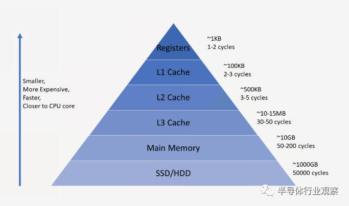
Memory Instructions and Hierarchy

For memory instructions, we need to understand a concept called “memory hierarchy.” This represents the relationship between cache, RAM, and main storage. When the CPU receives a memory instruction that targets data not yet stored locally in its registers, it will descend the memory hierarchy until it finds it. Most modern CPUs include three levels of cache: L1, L2, and L3. The first place the CPU checks is L1 cache. This is the smallest and fastest of the three levels of cache. L1 cache is typically divided into a section for data and a section for instructions. Remember, instructions need to be fetched from memory just like data.
A typical L1 cache might be a few hundred KB. If the CPU does not find the needed content in L1 cache, it will check L2 cache. This might be around a few MB. The next step is L3 cache, which might be dozens of MB. If the CPU does not find the needed data in any of the three caches, it will go to RAM, and finally to main storage. As we go down each step, the available space increases by about an order of magnitude, but the wait time also increases.
A Comprehensive Guide to CPU Architecture
Once the CPU finds the data, it will pull it from the hierarchy so that it can be quickly accessed again in the future if needed. There are many steps here, but the CPU can ensure that it quickly accesses the needed data. For example, the CPU can read its internal registers in one or two cycles, read L1 in several cycles, L2 in about ten cycles, and L3 in dozens of cycles. Accessing memory or main storage may take tens of thousands or even millions of cycles. Depending on the system, each core may have its own private L1 cache, share an L2 with another core, and share an L3 among four or more cores. We will discuss multi-core CPUs in more detail later in this article.

Branch and Jump Instructions

The last of the three main instruction types is the branch instruction. Modern programs endlessly jump around, and the CPU rarely executes a series of instructions without branches. Branch instructions come from programming elements like if statements, for loops, and return statements. These are used to interrupt program execution and switch to different parts of the code. There are also jump instructions, which are always taken branch instructions.
Conditional branches are particularly tricky for the CPU because it may execute multiple instructions at once, and it may not determine the outcome of the branch until after the branch has begun executing subsequent instructions.
To fully understand why this is a problem, we need to make another transition and discuss pipelining. Each step in the instruction cycle may take several cycles to complete. This means that while the instruction is being fetched, the ALU would otherwise be idle. To maximize the efficiency of the CPU, we divide each stage in a process called pipelining.
A classic way to understand this is by comparing it to doing laundry. You have two items to wash, and washing and drying each takes an hour. You can put the first item in the washer, then put it in the dryer, and wait for it to dry before starting the second item. This would take four hours. However, if you divide the work and start washing the second item while the first is drying, you can complete both loads in three hours. The hour saved depends on the number of items you have to wash and the number of washers and dryers you have. Each washing and drying still takes two hours, but by overlapping the calculations, you increase the total throughput from 0.5 items/hour to 0.75 items/hour.
A Comprehensive Guide to CPU Architecture
The CPU uses the same method to improve instruction throughput. Modern ARM or x86 CPUs may have more than 20 pipeline stages, meaning that at any given point, the core can handle more than 20 different instructions at once. Each design is unique, but a sample division might be 4 cycles for fetching, 6 cycles for decoding, 3 cycles for executing, and 7 cycles to update the results back to memory.
Back to branches, I hope you can start to see this problem. If it is not until cycle 10 that we know an instruction is a branch, we will have already started executing 9 new instructions that may be invalid if that branch is taken. To solve this problem, the CPU has a very complex structure called a branch predictor. They use concepts similar to those in machine learning to try to guess whether a branch will be taken. The complexity of branch prediction variables far exceeds the scope of this article, but at a basic level, they track the state of previous branches to understand whether an upcoming branch is likely to be taken. Modern branch predictors can achieve 95% accuracy or better.
Once the outcome of the branch is determined (the completed stage of the pipeline), the program counter is updated, and the CPU continues executing the next instruction. If the branch prediction was incorrect, the CPU will discard all instructions that were started after the branch was incorrectly taken, and then restart from the correct position.

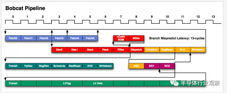
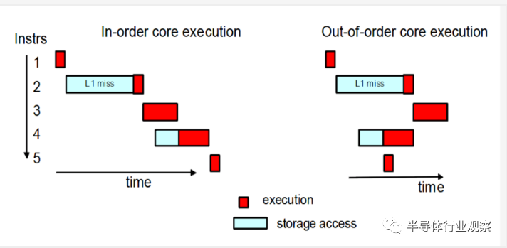
Out-of-Order Execution

Now that we know how to execute the three most common instruction types, let’s look at some more advanced features of the CPU. In reality, all modern processors do not execute instructions in the order they are received. They can use a technique called out-of-order execution to minimize downtime while waiting to execute other instructions.
If the CPU knows an upcoming instruction but the required data is not ready in time, it can switch the order of instructions and bring in an independent instruction from further down the program while it waits. This instruction reordering is a very powerful tool, but it is far from the only trick the CPU uses.
A Comprehensive Guide to CPU Architecture
Another performance-enhancing feature is called prefetching. If you were to time how long it takes to complete a random instruction from start to finish, you would find that memory access takes up most of the time. The prefetcher is a unit within the CPU that tries to anticipate future instructions and the data they will need. If it finds data that the CPU has not yet cached, it will reach out to RAM and pull that data into the cache. Hence, its name, prefetch.

Accelerators and the Future

Another major growing feature in CPUs is acceleration for specific tasks. These circuits are designed to complete a small task as quickly as possible. This may include encryption, media encoding, or machine learning.
The CPU can perform these tasks itself, but having dedicated units for them greatly improves efficiency. A dedicated GPU is a great example. The CPU can certainly perform the calculations needed for graphics processing, but equipping them with dedicated units can provide better performance by an order of magnitude. With the rise of accelerators, the actual cores of the CPU may only occupy a small portion of the chip.
The image below shows an Intel CPU from a few years ago. Most of the space is occupied by cores and cache. The second image below is a new AMD chip. Most of the space there is occupied by components outside of the cores.
A Comprehensive Guide to CPU Architecture

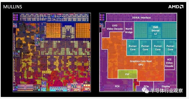
Moving to Multi-Core
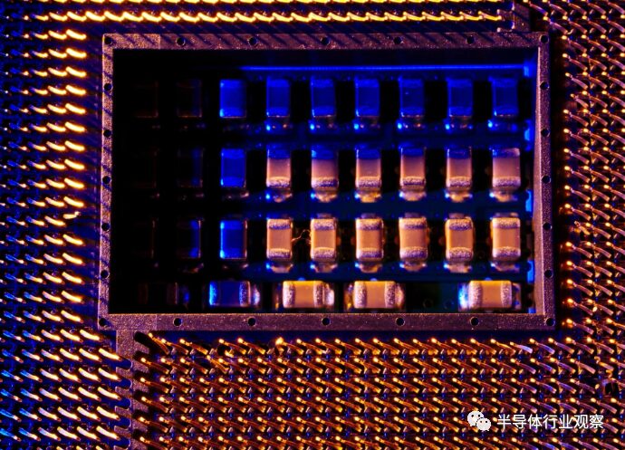
The last major feature to introduce is how to connect a bunch of individual CPUs together to form a multi-core CPU. This is not as simple as just putting multiple copies of the single-core design we discussed earlier. Just as there is no simple way to convert a single-threaded program into a multi-threaded one, the same concept applies to hardware. The problem arises from dependencies between cores.
For example, for a 4-core design, the CPU needs to be able to issue instructions at four times the speed. It also needs four separate memory interfaces. Since multiple entities may be processing the same data, issues like consistency and inconsistency must be addressed. If two cores are using the same data to process instructions, how do they know who has the correct value? What if one core modifies the data but that modification does not reach the other core in time to execute? Because they have separate caches that can store overlapping data, complex algorithms and controllers must be used to eliminate these conflicts.
As the number of cores in a CPU increases, correct branch prediction becomes very important. The more instructions that cores execute at once, the higher the likelihood that one of them will handle a branch instruction. This means that the instruction stream can change at any time.
Typically, separate cores will handle instruction streams from different threads. This helps reduce dependencies between cores. This is why if you check the “Task Manager,” you often see one core working hard while others are idle. Many programs are not designed for multi-threading. In some cases, letting one core do the work is much cheaper than paying the overhead of trying to share the workload.

Physical Design

Most of this article has focused on the architectural design of the CPU, as that is where most of the complexity lies. However, all of this needs to be realized in the real world, which adds another layer of complexity.
To synchronize all components within the processor, a clock signal is used. Modern processors typically run between 3.0GHz and 5.0GHz, and this has not changed much in the past decade. During each cycle, billions of transistors inside the chip switch on and off.
The clock is crucial for ensuring that all values are displayed at the correct time as each stage of the pipeline advances. The clock determines how many instructions the CPU can process per second. Increasing its frequency through overclocking will make the chip faster, but it will also increase power consumption and heat output.
A Comprehensive Guide to CPU Architecture
Heat is the CPU’s biggest enemy. As digital electronic devices heat up, microscopic transistors may start to degrade. Without dissipating heat, this could lead to chip damage. This is why all CPUs come with heat sinks. The actual silicon chip of the CPU may occupy only 20% of the physical device’s surface area. The increased space allows heat to dissipate more evenly to the heat sink. It also allows for more pins to interface with external components.
Modern CPUs can have thousands or more input and output pins on the back. Since most computational components are on-chip, a moving chip may have only a few hundred pins. Regardless of the design, about half of these are dedicated to power, while the rest are for data communication. This includes communication with RAM, chipsets, storage, PCIe devices, etc.
As high-performance CPUs draw 100 amperes or more of current under full load, they require hundreds of pins to evenly distribute current consumption. Pins are often gold-plated to improve conductivity. Different manufacturers use different pin arrangements across their many product lines.

Putting It All Together

To summarize, we will quickly introduce the design of the Intel Core 2 CPU. This is from 2006, so some parts may be outdated, but detailed information on newer designs is not yet available.
Starting from the top, we have the instruction cache and ITLB. The Translation Lookaside Buffer (TLB) helps the CPU know where to look for the required instructions in memory. These instructions are stored in the L1 instruction cache and then sent to the predecoder. The x86 architecture is extremely complex and dense, so there are many decoding steps. Meanwhile, the branch predictor and prefetcher are both anticipating any potential issues caused by incoming instructions.
A Comprehensive Guide to CPU Architecture
From there, the instructions are sent to the instruction queue. Remember how out-of-order designs allow the CPU to execute instructions and choose the most timely instruction to execute. This queue holds the current instructions the CPU is considering. Once the CPU knows which instruction will be the best to execute, it will further decode it into micro-operations. While an instruction may contain complex tasks for the CPU, micro-operations are fine tasks that the CPU can interpret more easily.
Then, these instructions enter the “registers,” “ROB,” and “reservation stations.” The exact functions of these three components are somewhat complex (think graduate-level university courses), but they are used in the out-of-order process to help manage dependencies between instructions.
A “core” will actually have many ALUs and memory ports. Incoming operations are placed in the reservation station until an ALU or memory port is available. Once the required components are available, the instruction will be processed with the help of the L1 data cache. The output result will be stored, and the CPU is now ready to start with the next instruction. That’s it!
While this article is not meant to guide exactly how every CPU works, it should give you a good understanding of how they operate internally and the complexities involved. Frankly, most people outside of AMD and Intel do not actually know how their CPUs work. Each part of this article represents an entire field of research and development, so the information provided here is just the beginning.

Public Account ID:imecas_wx

A Comprehensive Guide to CPU Architecture

Leave a Comment