 👆If you wish to meet regularly, feel free to star 🌟 and bookmark it~
The global chip industry may be on the brink of a revolutionary breakthrough! The research group led by Feng Jicheng at ShanghaiTech University (AIL) has successfully developed the world’s first “chip nano vessel 3D printer,” overcoming the processing bottleneck of next-generation interconnect metal materials—replacing traditional copper interconnects with next-generation materials like iridium and ruthenium, and achieving 3D bridge structures with a minimum feature size of 17 nm and wafer-level processing throughput (Figure 1). This domestically developed technology, named “Faraday 3D Printing,” reduces manufacturing energy consumption to one-millionth of traditional processes, providing strong support for the mass production of high-end domestic chips and breaking the dependence on imported equipment and materials.
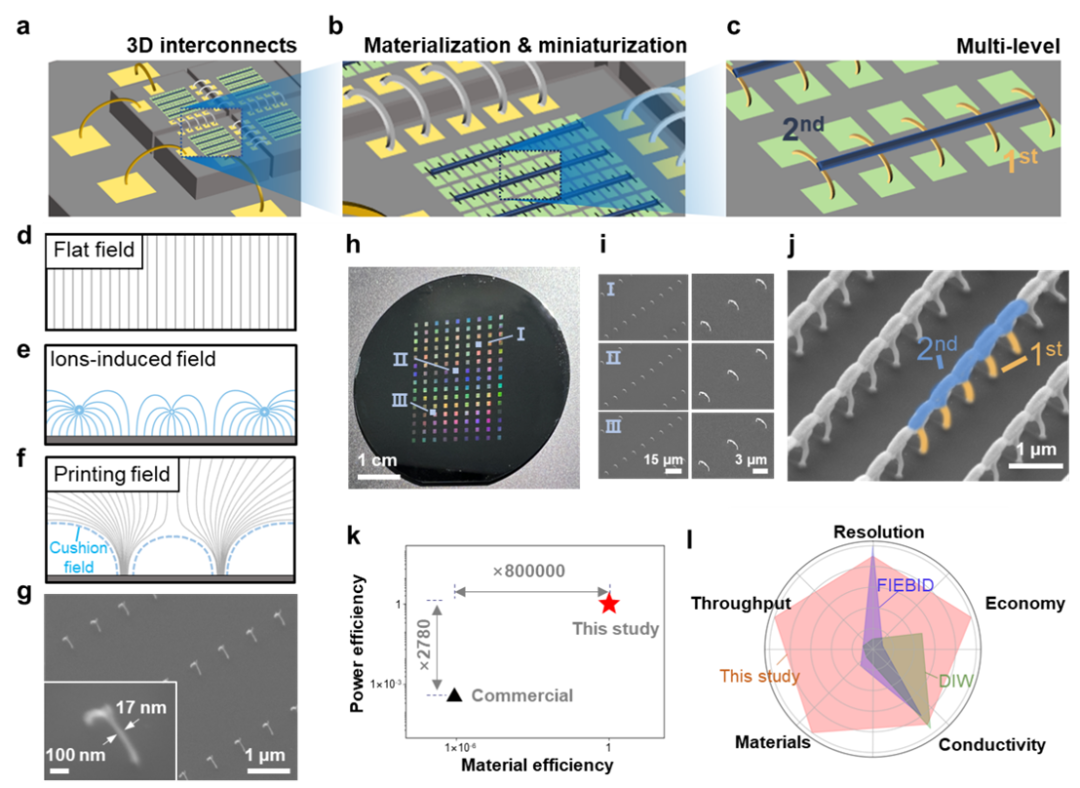
Figure 1. Faraday 3D printed wafer-scale large-area, multi-level, multi-scale, multi-material chip interconnect nano structures
Why is the “Nano Vessel Revolution” necessary?
Unveiling the next-generation interconnect metal materials
Billions of “metal vessels” inside chips are facing a life-and-death crisis! The copper interconnects relied upon by high-end chips, when the line width shrinks below 10 nm, behave like “rusty pipes”—the resistivity increases by 300%, causing severe heating and even failure, directly hindering performance enhancement. Materials like iridium and ruthenium are considered the “next-generation interconnect metal materials” due to their weak resistance size effect (Figure 2).However, since most next-generation interconnect materials are precious metals and the mainstream Damascus process cannot fully adapt, these materials have not yet made their debut in actual chips.
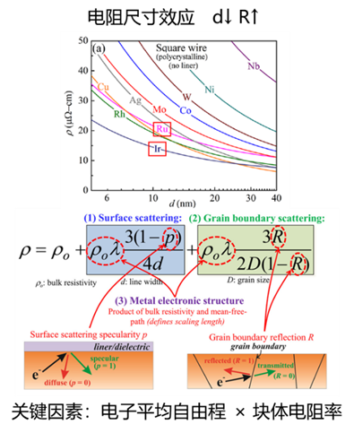
Figure 2. Main properties of next-generation interconnect metal materials:
Resisting the resistance size effect
Future industry disruptors
In addition to solving the processing challenges of next-generation interconnect metal materials, Feng Jicheng’s research group has endowed their self-developed nano-printing technology with four key characteristics, allowing it to directly interface with integrated circuit processes:
-
Cost reduction: Material usage is only 0.0001% of traditional processes, with energy consumption savings of 99.9% (Figure 1), enabling small and medium chip manufacturers to utilize expensive next-generation materials;
-
Superior performance: After simple heat treatment, the 3D printed metal interconnect structures can exhibit performance close to theoretical predictions (Figure 3);
-
Wafer-level throughput: A single print can process over 10,000,000 3D nano structures in a wafer-scale large-area array within 60 minutes (Figure 4);
-
Domestic breakthrough: The core technology has applied for 19 invention patents, and once domestic equipment is mass-produced, it can completely eliminate dependence on foreign equipment.
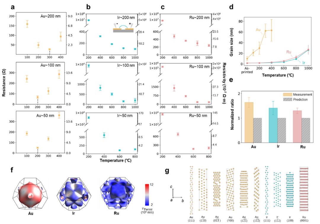
Figure 3. The performance of Faraday 3D printed interconnect structures approaches theoretical values.
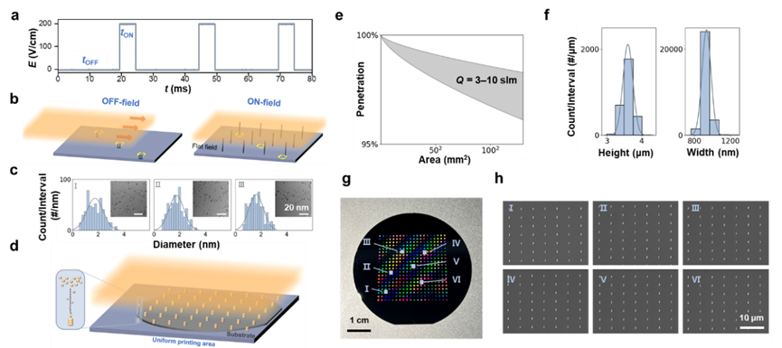
Figure 4. The research team developed a wafer-scale high-throughput Faraday 3D printing based on pulsed electric fields, capable of printing wafer-scale nano structure arrays within one hour.
The work presented above demonstrates the application potential of printing three-dimensional nano structures as chip interconnects, promising new development opportunities for interconnect solutions that are constrained by existing manufacturing methods. Meanwhile, this technology is not only applicable to integrated circuit interconnect manufacturing and metallization but also shows broad application prospects in cutting-edge fields such as MEMS and optical metamaterials (Research Progress | Feng Jicheng’s group at ShanghaiTech University published a cover article in Advanced Materials: 4D printing of colored micro films, with the self-developed “power line brush” rapidly depicting multi-material, high-precision three-dimensional nano structure arrays). Looking ahead, Feng Jicheng’s team will continue to delve into the industrial application research of nano-scale 3D printing technology, focusing on promoting the deep integration of this technology with existing chip manufacturing processes, aiming to tackle the “bottleneck” technical challenges that restrict the development of China’s integrated circuit industry and inject new momentum into enhancing China’s independent innovation capabilities in high-end chip manufacturing.
Related research results titled “Wafer-scale nanoprinting of 3D interconnects beyond Cu” were published in the international academic journalACS NANO, and selected as a Supplementary Cover achievement. ShanghaiTech University is the sole completing unit for this achievement.
Paper title: Wafer-scale nanoprinting of 3D interconnects beyond Cu
Paper link: https://pubs.acs.org/doi/10.1021/acsnano.5c00720xxxxxx
Key points
As the mainstream copper interconnect processes battle in a red ocean, a new force has torn open a new track for next-generation chip interconnects with a “nano vessel revolution.” Comprehensive autonomy from materials, equipment to processes may be a feasible path for China’s semiconductor industry to break through the “bottleneck” dilemma.
For cooperation, please contact
Team website: http://www.jcfenglab.com
ShanghaiTech Technology Transfer Office, email: [email protected]
END
👇 Recommended Semiconductor Quality Public Account 👇
▲ Click the card above to follow
Focusing on more original content in the semiconductor field
▲ Click the card above to follow
Follow global semiconductor industry trends and movements
*Disclaimer: This article is original by the author. The content reflects the author’s personal views, and Semiconductor Industry Observation reprints it only to convey a different perspective, not representing endorsement or support for that view. If there are any objections, please contact Semiconductor Industry Observation.

Today is the 4021th issue shared by “Semiconductor Industry Observation”. Welcome to follow.
Recommended Reading
★A chip that changed the world
★U.S. Secretary of Commerce: Huawei’s chips are not that advanced
★“ASML’s new lithography machine is too expensive!”
★The quietly rising new competitor of NVIDIA
★Chip prices plummet, all blame on Trump
★New alternatives to EUV lithography announced!
★Semiconductor equipment giants see a 40% salary increase
★Foreign media: The U.S. will propose banning software and hardware made in China for automobiles


『Semiconductor’s First Vertical Media』
Real-time Professional Original Depth
Public Account ID: icbank
If you like our content, please click“Looking” to share with your friends!