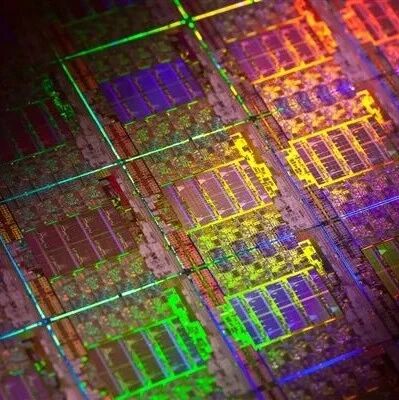
Reconstructing the Semiconductor Industry Landscape: Opportunities and Challenges of Wafer Fab Location Recognition

Reconstructing the Semiconductor Industry Landscape: Opportunities and Challenges of Wafer Fab Location Recognition

1. Policy Background and Essence of the Rules On April 11, 2025, the China Semiconductor Industry Association issued an urgent notice clarifying that the origin of integrated circuits is determined by the “wafer fab location”. This rule is not a new policy but a reiteration and refinement of the long-standing “four-digit tariff number change principle” … Read more

Analysis of ‘Wafer Fabrication as Origin’ – Opportunities for Semiconductor Self-Control (Including Comprehensive Industry Chain Overview)

Analysis of 'Wafer Fabrication as Origin' - Opportunities for Semiconductor Self-Control (Including Comprehensive Industry Chain Overview)

Previous Recommendations China-Europe Cooperation, Core Beneficiary Industry Chain Overview Comprehensive Tariff Countermeasures, Detailed Overview of 9 Beneficial Concepts Striking a Blow to Avoid a Hundred Blows: An Overview of Opportunities in Tariff Countermeasures! Active Countermeasures Against Tariff Increases by Penicillin, The Most Authentic 6 Companies In-Depth Analysis of Controlled Nuclear Fusion Expectations, The Most Authentic … Read more

Services | AMF Silicon-based Nitride (PESiN-on-SOI) Wafer Fabrication Services

Services | AMF Silicon-based Nitride (PESiN-on-SOI) Wafer Fabrication Services

2025/03/22, Advanced Photonics Based on AMF’s latest Process Design Kit (PDK4.5) PESiN-on-SOI wafer fabrication process (process capabilities are backward compatible), Xiaoguang regularly organizes silicon-based photonic chip wafer fabrication services, providing a full-process solution from design to delivery: 1) Design Services: Photonic integrated components, system simulation, and design; 2) Layout Services: Layout drawing and review in … Read more

Texas Instruments’ New 12-Inch Wafer Manufacturing Facility in Lehi, Utah Begins Production

Texas Instruments' New 12-Inch Wafer Manufacturing Facility in Lehi, Utah Begins Production

Click the blue text above Follow us! Texas Instruments’ new 12-inch wafer fab LFAB in Lehi, Utah has begun production of analog and embedded products, approximately one year after the company acquired the facility. LFAB is our second 12-inch wafer fab to begin semiconductor production in 2022, providing our customers with the manufacturing capacity needed … Read more

What is the NRE Stage of MEMS Wafer Fabrication? What is the Relationship Between MPW and NRE?

What is the NRE Stage of MEMS Wafer Fabrication? What is the Relationship Between MPW and NRE?

Source: Chip Learning Original Author: Chip Future The semiconductor wafer fabrication NRE refers to “Non-Recurring Engineering” costs, which are one-time expenses incurred during the chip development process. These costs cover a series of non-recurring work from chip design to the successful first wafer fabrication, including design and R&D expenses, mask production costs, process development and … Read more

In-Depth Analysis of Eight Major Chip Materials

In-Depth Analysis of Eight Major Chip Materials

CCTC® Click the blue text above to follow Brief Overview: Source: Future Think Tank Hua Xia Climate 30,000+ fans,Welcome to place commercial advertisements, prices are beautiful Thank you for your recognition and support! Processed wafers from foundries Chip design diagram Coating photoresist Photo mask Principle of wafer exposure Photo lithography machine for wafer exposure Internal … Read more