Overview
The Xilinx white paper WP272 “Get Smart About Reset: Think Local, Not Global” details the global reset of FPGAs. In digital system design, we traditionally believe that a reset signal should be set for all flip-flops, which greatly facilitates subsequent testing. Therefore, when the document mentions that “global reset is not recommended in FPGA design, or that efforts should be made to avoid this design approach,” many designers find it very difficult to understand, as this design philosophy conflicts with our usual understanding.
Xilinx Reset Guidelines
Minimize the use of resets, especially global resets; if a reset is not necessary, do not use it. If a reset must be used, prefer local resets over global resets.
If a reset is necessary, use synchronous resets whenever possible, and if asynchronous resets must be used, adopt “asynchronous reset, synchronous release”.
Choose a high-level reset signal. (Note: Due to the different internal structures of Altera and Xilinx devices, Altera’s FPGAs recommend low-level resets.)
Global resets can be implemented in the following three ways:
1. Use a reset button to generate a reset signal connected to the FPGA’s global reset pin; its speed is very slow (in milliseconds), and the reset time is uncertain.
2. At power-up, the power chip generates a reset signal, such as the TI TPS76x series power chips, which can generally produce a reset signal for the main chip’s power-on reset. The control chip generates reset pulses, which are convenient for designers to control programmatically.
In these cases, the change of the reset signal is extremely slow compared to the internal signals of the FPGA chip; for example, the period of the reset signal generated by the reset button is at least in the millisecond range, while the internal signals of the FPGA are often in the nanosecond or microsecond range. The frequency of the reset signal is so low that we consider it not timing-critical. Even if timing constraints are applied to such signals, the constraint period is very long. The period of the global reset pulse is much greater than the clock period, so it is traditionally believed that all flip-flops in the FPGA chip can receive effective resets.
However, as FPGA performance and operating frequency rapidly increase, this assumption begins to break down. At this point, the generation of the global reset signal starts to become a timing-critical issue.
In Xilinx FPGA devices, the global reset/set signal (Global Set/Reset (GSR)) (which can be introduced through the global reset pin) is very reliable because it is an internal chip signal. If all flip-flops use this global reset signal, the GSR signal will form a high fan-out network. Although it can be synchronized with a user-defined clock during the startup sequence, it is impossible to synchronize it with all clock signals in the design; for example, a Xilinx FPGA may contain multiple DLL/DCM/PLL clock processing modules, each of which can generate multiple clock signals. Synchronizing clock signals within each module is feasible, but synchronizing all clock signals is completely impractical—this is evident from the distribution of DCMs: the long-distance wiring between them significantly increases the delay for high-frequency clock signals, making synchronization impossible. Thus, as clock signal frequencies increase, the global reset signal begins to become timing-critical. The explanation is as follows:
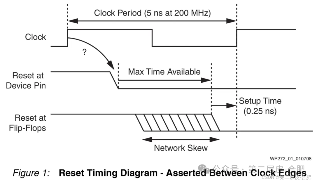
Timing diagram of the reset signal between two clock edges
The above diagram shows the timing diagram of the reset signal truncated by the edges of two clock signals. The first row is the clock signal, the second row is the signal on the device reset pin, and the third row is the reset signal reaching the reset input of the flip-flop. To effectively reset the flip-flop, the reset signal should be held for at least one setup time (the setup time of the clock signal) before the valid clock edge arrives. It can be seen that the higher the frequency of the clock signal, the less available time there is to distribute the reset signal. Moreover, considering that the global reset signal is often a high fan-out network, it is very difficult to meet stringent timing requirements in this large network. In commonly used asynchronous reset designs, it is even more impossible to guarantee that all flip-flops can be released on the same clock edge, even if there is available time to distribute the reset signal. This is evident from Figure 2.
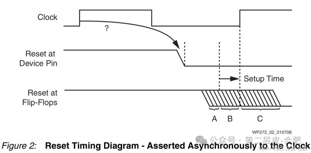
Timing diagram of the reset signal in asynchronous design
Figure 2 shows the timing diagram of the reset signal in asynchronous design. It can be seen that the reset signal generated at time A will occur at the valid edge of the first clock signal, while the reset signal generated at time C will occur at the valid edge of the second clock signal. At time B, it is difficult for the flip-flop to effectively define which reset signal is valid, which will lead to metastability.
As the frequency of the clock signal increases and the potential clock skew caused by the larger device scale, it has become almost impossible to reset all flip-flops on the same clock edge. Figure 3 shows the reset timing diagram at high clock frequencies.
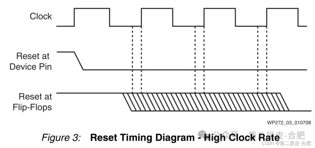
Reset timing at high clock frequencies
Is the timing requirement for global reset really critical?
The good news is that in the vast majority of designs (the white paper states over 99.99%), the timing of the reset signal is not critical—generally, most circuits can operate normally. However, if you have ever encountered a situation where the abnormal reset signal caused the circuit to malfunction, then you can say you have “luckily” encountered that 0.01% of abnormal reset signal cases. Figure 4 shows a case of pipeline reset.
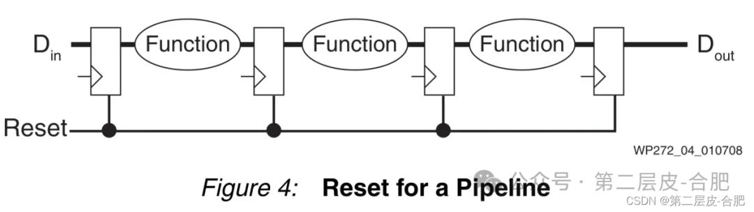
Pipeline Reset
In a pipeline, if the data is processed in a completely sequential manner (i.e., there are no feedback loops, etc.), then the timing of when the main reset signal is generated is completely irrelevant. After several cycles of pipeline operation, any abnormal data state will be “flushed out” of the pipeline, which is easy to understand. In fact, during normal pipeline operations, we rarely use reset operations because it is completely unnecessary. Even in simulation environments, we often configure the initial state in the test program to clear all unknown states from the system, making all inputs in the system valid data.
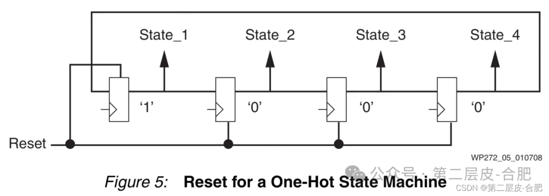
However, in the case of the one-hot state machine shown in Figure 5, the timing of the reset signal indeed becomes one of the critical factors for the system to operate normally.