
Click the “blue text” to follow us for more information
Research Background
All-perovskite tandem solar cells (TSCs) exhibit outstanding performance and broad application prospects. However, a significant challenge remains in narrowing the power conversion efficiency (PCE) gap between small-area and large-area (>1 cm²) devices, which has become a major obstacle to the commercialization of all-perovskite TSCs.
Research Content
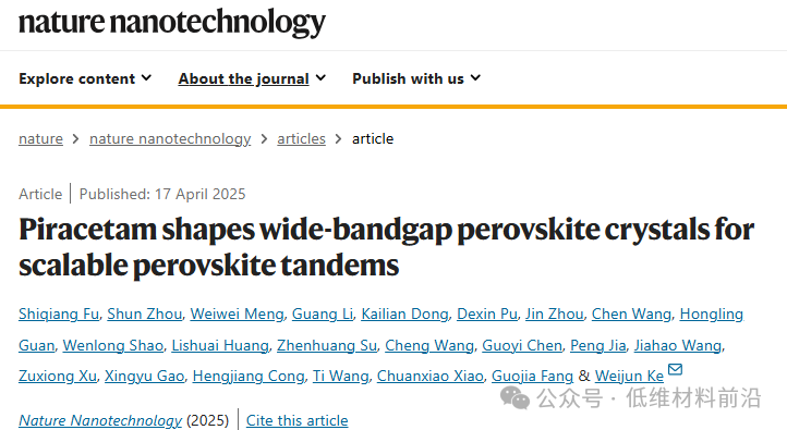
Here, Professor Ke Weijun’s team from the School of Physics Science and Technology at Wuhan University published a paper titled “Piracetam shapes wide-bandgap perovskite crystals for scalable perovskite tandems” in the journal Nature Nanotechnology. This paper introduces a crystal modifier specifically for wide-bandgap perovskite—piracetam, which promotes the construction of efficient large-area TSCs by homogenizing the top wide-bandgap sub-cell. Piracetam contains amide and pyrrolidone groups, which can first regulate the nucleation of perovskite, forming large-sized grains, preferential (110) orientation, enhanced crystallinity, and uniform optoelectronic properties.
During the subsequent annealing process, it further eliminates residual PbI2 and promotes the formation of one-dimensional (Pi) PbI3 (Pi = piracetam) perovskite nanoneedles, primarily distributed at grain boundaries and surfaces. As a result, the single-junction 1.77 eV bandgap solar cell achieved a certified open-circuit voltage of 1.36 V and a PCE of 20.35%. Furthermore, our single-ended all-perovskite TSCs achieved PCEs of 28.71% (stable value 28.55%, certified value 28.13%) and 28.20% (stable value 28.05%, certified value 27.30%) at aperture sizes of 0.07 cm² and 1.02 cm², respectively, with minimal PCE loss of only 0.51% during the transition from small-area to large-area devices.
Additionally, piracetam demonstrated broad applicability across different perovskite compositions, enhancing the PCE of the single-junction 1.56 eV bandgap solar cell from 23.56% to 25.71%. This method provides an effective production pathway for large-scale, high-efficiency all-perovskite TSCs.
Illustrated Summary
1. The experiment first introduced the crystal modifier—piracetam, successfully regulating the nucleation process of wide-bandgap (WBG) perovskite, resulting in large-sized grains, preferential (110) orientation, enhanced crystallinity, and uniform optoelectronic properties.
2. The experiment improved the crystal quality of WBG perovskite by forming one-dimensional (Pi) PbI3 perovskite nanoneedles at grain boundaries through the reaction of piracetam with PbI2, significantly reducing defects and enhancing optoelectronic performance.
3. The results indicated that the single-junction 1.77 eV bandgap solar cell achieved a certified open-circuit voltage (Voc) of 1.36 V and a PCE of 20.35%.
4. In the two-terminal (2T) all-perovskite tandem solar cells, the small-area 0.07 cm² and large-area 1.02 cm² devices achieved PCEs of 28.71% (certified value 28.13%) and 28.20% (certified value 27.30%), respectively, demonstrating minimal PCE loss of only 0.51% during the transition from small-area to large-area devices.
5. Piracetam also exhibited broad applicability, improving the PCE of different perovskite compositions, raising the PCE of the 1.56 eV bandgap single-junction solar cell from 23.56% to 25.71%.
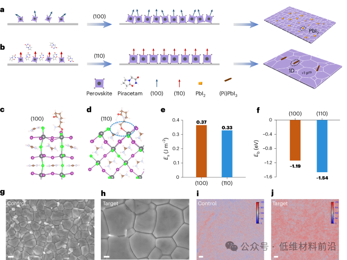
Figure 1 | Schematic diagram of the effect of piracetam on wide-bandgap perovskite.
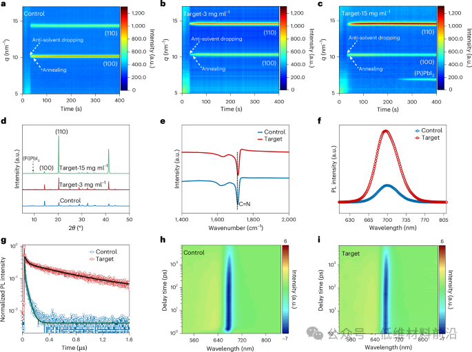
Figure 2 | The effect of piracetam on wide-bandgap perovskite thin film crystals.
Figure 3 | The effect of piracetam on all-perovskite stacked cells.
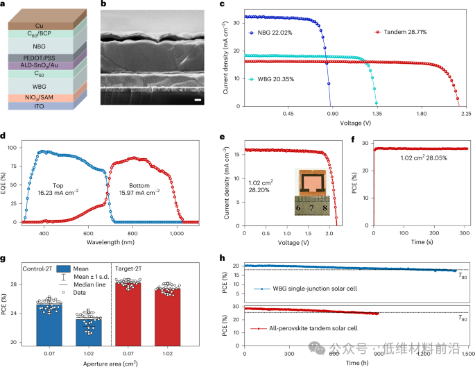
Figure 4 | Performance of 2T all-perovskite tandem solar cells.
Conclusion and Outlook
This paper effectively improves the crystal quality of wide-bandgap (WBG) perovskite thin films by introducing piracetam as a crystal modifier, reducing defects, enhancing crystallinity, and forming one-dimensional (Pi) PbI3 perovskite nanoneedles, significantly enhancing the optoelectronic performance of the devices. This method not only reduces open-circuit voltage (Voc) loss but also significantly increases PCE, particularly narrowing the efficiency gap between small-area and large-area devices, which is crucial for promoting the commercialization of all-perovskite TSCs. Furthermore, this study reveals the key role of the uniformity and crystal growth mechanism of perovskite films in the preparation of large-area high-efficiency devices. Nevertheless, facing issues such as phase separation and ion migration in large-area tandem modules, further optimization of WBG sub-cell materials, NBG sub-cells without PEDOT:PSS, and tunneling layer design technologies is needed in the future. Therefore, combining advanced interface engineering strategies with scalable fabrication techniques will be a key direction for enhancing the performance of all-perovskite tandem solar cells.
This work was published in Nature Nanotechnology.
Article link (click “Read the original text”): https://doi.org/10.1038/s41565-025-01899-z
Disclaimer | Some materials are sourced from the internet. Due to the author’s limited knowledge, please leave comments for corrections if there are any omissions or errors. If there are any infringements, please contact us for resolution.

Recently Popular Materials
MoS2 | WTe2 | MoSe2 | CuInP2S6 | 2H-MoTe2 | Black Phosphorus | α-In2Se3
Product Manual
“Online Product Manual for Low-Dimensional Materials”


Product Consultation
Chen Guyi – Junna Group Low-Dimensional Materials Online
Phone|13651969369
Email|[email protected]

Long Press to Follow
Low-Dimensional Materials Online Mall
Phone|021-56830191, 56830192
Email|[email protected]
Professionally ProvidingLow-Dimensional Materials as a Representativeof
Full Range of Laboratory Consumables and Tools

Click the “Read the original text” below to enter the original link
↓↓↓