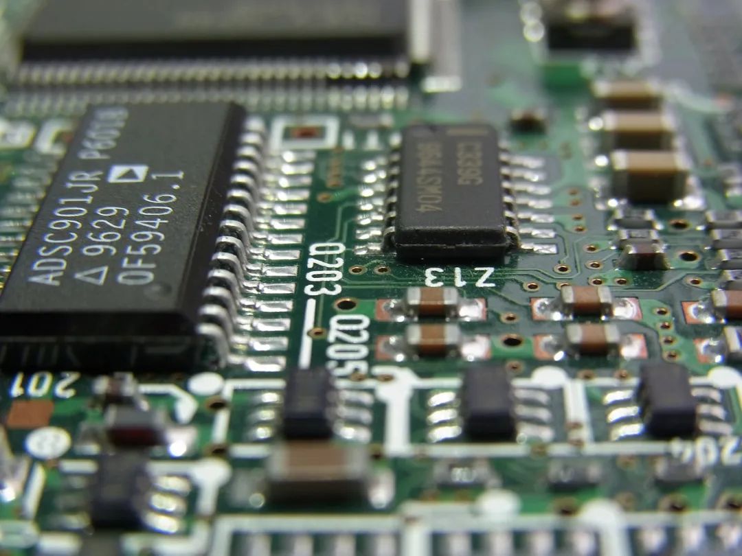
In the field of electronic engineering, printed circuit boards (PCBs) are indispensable components that carry the connections and communication between electronic components. A PCB is not a single-layer structure; it is composed of multiple layers, each with its specific functions and roles. Let’s discuss them below.

1. Mechanical Layer Definition: The mechanical layer represents the overall appearance and dimensions of the PCB. Function: It defines the boundaries, dimensions, assembly instructions, and other information related to mechanical characteristics of the circuit board. Usage Notes: The mechanical layer is often displayed together with other layers but should not be used for electrical routing.
2. Keep Out Layer Definition: This layer defines the areas on the PCB where routing or placement of components is allowed. Function: By drawing closed areas, it sets boundaries for automated layout and routing, ensuring the effectiveness of the circuit design. Usage Notes: The keep-out layer should not be confused with the mechanical layer, and its boundaries define the scope of electrical routing.
3. Signal Layer Definition: The signal layer is the area on the PCB used for routing traces, including the top layer, bottom layer, and mid-layers. Function: The top and bottom layers are typically used for placing components, while the mid-layers are used for routing, establishing electrical connections between components. Number of Layers: Depending on design requirements, a PCB can have multiple mid-layers for complex routing designs.4. Top Paste and Bottom Paste Definition: These two layers represent the solder paste stencil layers for the top and bottom sides. Function: In SMT (Surface Mount Technology), the top paste and bottom paste layers are used to create stencils, ensuring even application of solder paste, thus optimizing the soldering process. Application: The holes in the stencil match the size of the pads, ensuring that solder paste can be accurately applied to the pads.