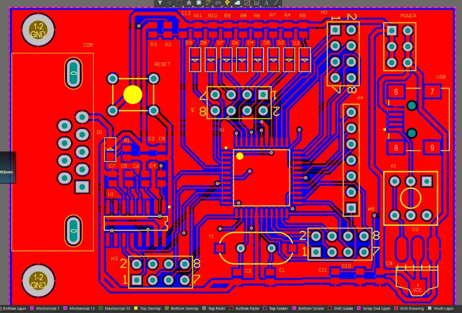
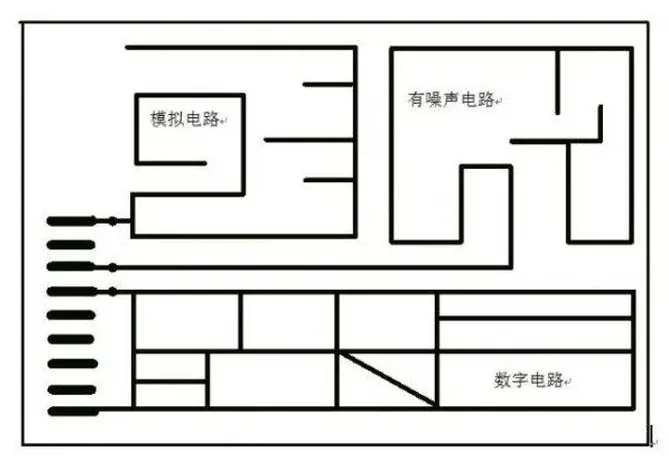
(1) Pre-define digital, analog, and DAA signal wiring areas on the PCB.
(2) Separate digital and analog components and their respective traces as much as possible, placing them in their designated wiring areas.
(3) Keep high-speed digital signal traces as short as possible.
(4) Keep sensitive analog signal traces as short as possible.
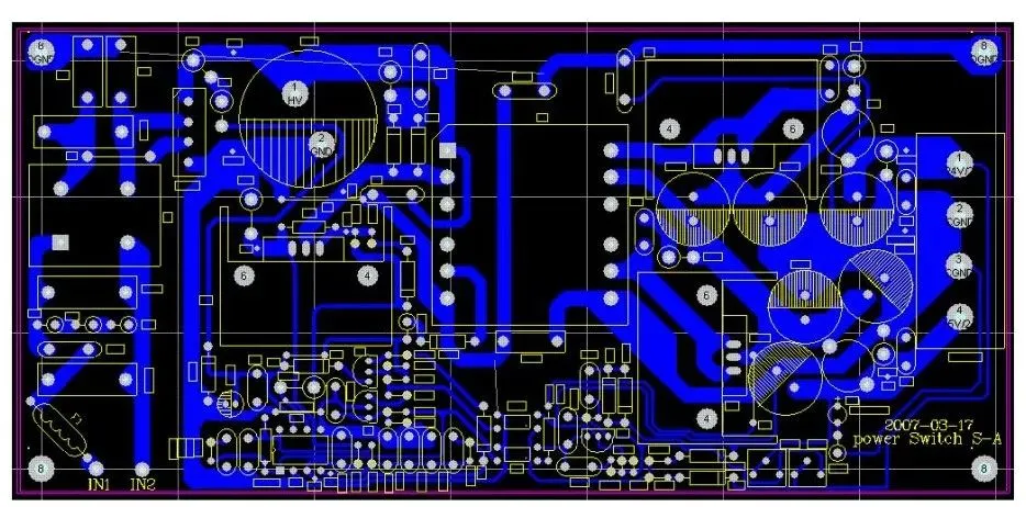
(5) Allocate power and ground reasonably.
(6) Separate DGND, AGND, and real ground.
(7) Use wide traces for power and critical signal wiring.
(8) Power and ground lines should be as radial as possible, and signal lines should not have looped traces.
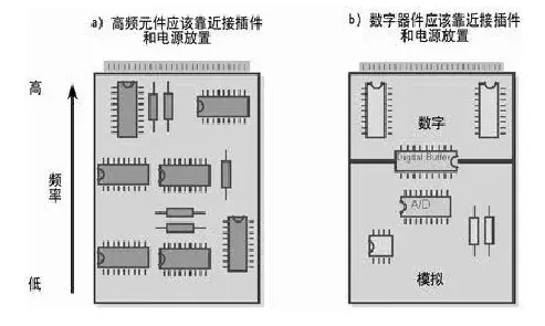
(9) Place digital circuits near parallel bus/serial DTE interfaces, and DAA circuits near telephone line interfaces.
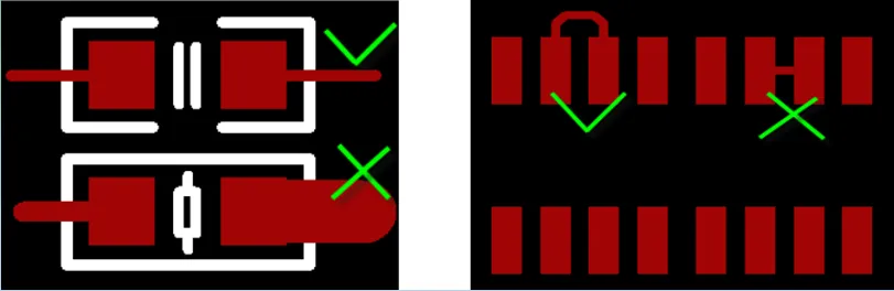
(10) Small discrete component traces must be symmetrical, and closely spaced SMT pad leads should connect from outside the pads, not directly in the middle of the pads.
(11) Prioritize critical signal lines: Power, small analog signals, high-speed signals, clock signals, and synchronization signals are prioritized.
(12) Wiring density prioritization principle: Start wiring from the components with the most complex connections on the board. Begin wiring from the areas with the densest connections on the board.
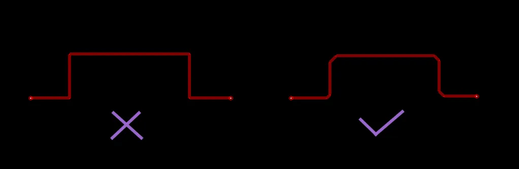
(13) Avoid sharp angles and right angles in PCB design to prevent unnecessary radiation, as well as poor PCB manufacturing performance.
(14) There should be no through-holes on the surface mount pads to prevent solder paste loss, causing component cold soldering. Important signal lines must not pass between pin connections.
High-Frequency Circuit Wiring on PCB
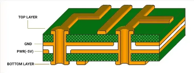
(1) Reasonably choose the number of PCB layers. Using an intermediate power layer (VCC layer) and ground layer (GND layer) can provide shielding, effectively reducing parasitic inductance and capacitance, and can significantly shorten wiring length, reducing signal interference.
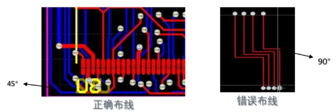
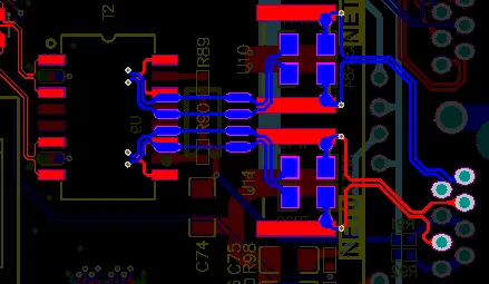
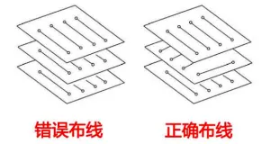
(2) Wiring method: Must use 45° angles, avoid 90° angles. As shown in the figure:
(3) Inter-layer wiring direction: should be mutually perpendicular, with the top layer horizontal and the bottom layer vertical, which can reduce signal interference.
(4) Grounding: Grounding important signals can significantly improve the signal’s anti-interference ability, and grounding multiple interference signals can prevent them from interfering with other signals.
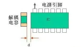
(5) Decoupling capacitors: Add decoupling capacitors at the power supply end of the IC.
(6) High-frequency choke: When there are common grounds like digital ground and analog ground, add high-frequency choke devices between them, typically using high-frequency ferrite beads with a wire passing through the center hole.
(7) Copper pouring: Increasing the area of grounding can also reduce signal interference. (During copper pouring, dead copper must be removed.)
(8) Trace length: The shorter the trace length, the better, as this will reduce interference. However, not all traces should only pursue shortness, such as DDR traces, which emphasize equal lengths between clock, address, and data traces, hence the presence of serpentine traces designed to increase length.
Wiring for Special Components
(1) High-frequency components: The shorter the connection between high-frequency components, the better, attempt to reduce the distributed parameters and mutual electrical interference between connections, and components that are prone to interference should not be too close.
(2) Components with high potential difference: Increase the distance between components with high potential difference and their connections to avoid accidental short circuits that could damage components. To prevent creeping discharge, the distance between copper foil lines with a potential difference of 2000V should generally exceed 2mm.
(3) Heavy components: Overly heavy components should be secured with a bracket.
(4) Heating and temperature-sensitive components: Ensure heating components are kept away from temperature-sensitive components. High-heat components should be evenly distributed.
Important Parameters for PCB Wiring Design
(1) Copper track width: Single-sided board 0.3mm, double-sided board 0.2mm;
(2) Minimum gap between copper foil lines: single-sided board 0.3mm, double-sided board 0.2mm;
(3) Minimum distance of copper foil lines from PCB edge is 1mm, components from PCB edge is 5mm, pads from PCB edge is 4mm;
(4) The diameter of pads for through-hole mounted components is generally twice the inner diameter of the pads.
(5) Electrolytic capacitors should not be placed near heating components, such as high-power resistors, transformers, high-power transistors, three-terminal voltage regulators, and heat sinks. The distance between electrolytic capacitors and these components should not be less than 10mm.
(6) There should be no copper foil lines (except for grounding) and components within 5mm radius of screw holes.
(7) In large area PCB designs (over 500㎡), to prevent bending during wave soldering, leave a gap of 5mm to 10mm in the middle of the PCB to place braces to prevent bending.
(8) Each PCB should have a hollow arrow indicating the direction of wave soldering.
(9) When wiring DIP packaged ICs, the orientation should be perpendicular to the direction of wave soldering, and parallel placement should be avoided to prevent solder bridging.
(10) When changing from vertical to horizontal wiring direction, it should enter from a 45° angle.
(11) Power line width should not be less than 18mil; signal line width should not be less than 12mil; CPU input/output line should not be less than 10mil (or 8mil); line spacing should not be less than 10mil.
(12) Wiring on the board should be appropriately dense; if the density difference is too large, it should be filled with mesh copper foil, with a grid size greater than 8mil (or 0.2mm).
(13) Wiring is prohibited within the area ≤1mm from the defined wiring area to the PCB edge, and within 1mm around mounting holes.
(14) Areas with components such as fuses, fusible resistors, AC220V filter capacitors, transformers, etc., should have warning marks printed on the silkscreen layer.
(15) The distance between the live wire and neutral wire in the AC220V power section should not be less than 3mm. Any wire in the 220V circuit should have a distance of not less than 6mm from low-voltage components and pads, tracks, and should be marked for high voltage, with a thick silkscreen line separating weak and strong current to warn maintenance personnel to exercise caution.
Copyright Notice: This article’s copyright belongs to the original author and does not represent the association’s views. Articles promoted by the “Jiangxi Province Electronic Circuit Industry Association” are for sharing purposes only and do not represent this account’s stance. If there are any copyright issues, please contact us for removal.