In the previous article, Xiaozhao introduced CPU and GPU. Today, I will continue to introduce two other main characters in the field of computing chips—ASIC and FPGA.█ ASIC (Application Specific Integrated Circuit) As mentioned earlier, GPUs have strong parallel computing capabilities, but they also have disadvantages, such as high power consumption, large size, and high cost.Entering the 21st century, the demand for computing power has shown two significant trends: first, the usage scenarios for computing power have started to diversify; second, users’ requirements for computing power performance are increasingly high. General-purpose computing chips can no longer meet user needs.As a result, more and more companies are strengthening their research and investment in dedicated computing chips. ASIC (Application Specific Integrated Circuit) is a type of chip specifically designed for specific tasks. The official definition of ASIC is: integrated circuits designed and manufactured specifically to meet the requirements of specific users or the needs of specific electronic systems.ASIC started in the 1970s and 1980s. In the early days, it was used for computers. Later, it was mainly used for embedded control. In recent years, as mentioned earlier, it has begun to rise for applications such as AI inference, high-speed search, and visual and image processing.Speaking of ASIC, we must mention Google’s famous TPU.
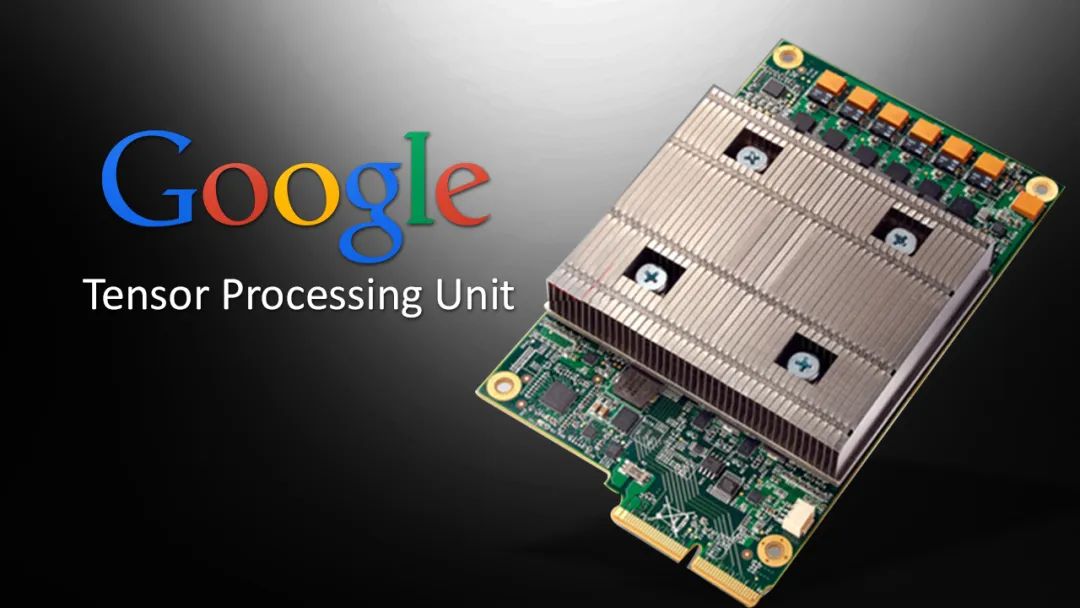 TPU, short for Tensor Processing Unit, is a tensor processing unit. The term “tensor” refers to a mathematical entity that contains multiple numbers (multi-dimensional arrays).Currently, almost all machine learning systems use tensors as the basic data structure. Therefore, we can simply understand the tensor processing unit as an “AI processing unit”.In 2015, to better accomplish its deep learning tasks and enhance AI computing power, Google launched a chip specifically for neural network training, namely TPU v1.
Compared to traditional CPU and GPU, TPU v1 can achieve a performance improvement of 15 to 30 times in neural network computing, with energy efficiency increasing by 30 to 80 times, bringing a significant impact to the industry.
In 2017 and 2018, Google continued to improve, launching more powerful TPU v2 and TPU v3 for AI training and inference. In 2021, they released TPU v4, which uses a 7nm process and has a transistor count of 22 billion, with performance improved by 10 times compared to the previous generation, outperforming NVIDIA’s A100 by 1.7 times.
In addition to Google, many large companies have also been working on ASIC in recent years.Intel acquired the Israeli AI chip company Habana Labs at the end of 2019, and in 2022, released the Gaudi 2 ASIC chip. IBM Research released the AI ASIC chip AIU at the end of 2022.Samsung also worked on ASIC a few years ago, specifically for mining machines. Indeed, many people associate ASIC with Bitcoin mining. Compared to GPU and CPU mining, ASIC mining machines are more efficient and consume less power.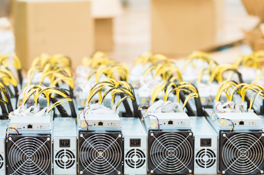 ASIC mining machinesAside from TPU and mining machines, two other well-known types of ASIC chips are DPU and NPU.DPU stands for Data Processing Unit, primarily used in data centers. Xiaozhao previously introduced it specifically; you can check it out here: What Is DPU That Is Popular Online?NPU, or Neural Processing Unit, simulates human neurons and synapses at the circuit level and processes data using a deep learning instruction set.NPU is specifically used for neural network inference, capable of efficiently performing operations like convolution and pooling. It is often integrated into smartphone chips.Speaking of smartphone chips, it’s worth mentioning that the main chip in our phones, commonly referred to as the SoC chip, is also a type of ASIC chip.
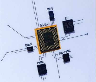 Smartphone SoC chipWhat are the advantages of ASIC as a dedicated custom chip? Is it just that enterprises enjoy exclusive logos and naming?No.Customization means tailoring to specific needs. Based on the specific tasks the chip is designed for, the chip’s computing power and efficiency are strictly matched to the task algorithms. The number of cores, the ratio of logic computing units and control units, as well as cache, and the entire chip architecture are all precisely customized.Thus, custom dedicated chips can achieve extreme compactness and low power consumption. The reliability, confidentiality, computing power, and energy efficiency of these chips are all stronger than general-purpose chips (CPU, GPU).You will notice that several ASIC companies mentioned earlier are all large firms like Google, Intel, IBM, and Samsung.
This is because custom chip design requires a very high level of R&D technical capability and is extremely costly.
To make an ASIC chip, one must first go through complex design processes such as code design, synthesis, and backend processes, followed by several months of production and packaging testing before the chip can be obtained to build a system.Everyone has heard of “tape-out”. Like an assembly line, manufacturing chips through a series of process steps is tape-out. In simple terms, it is trial production.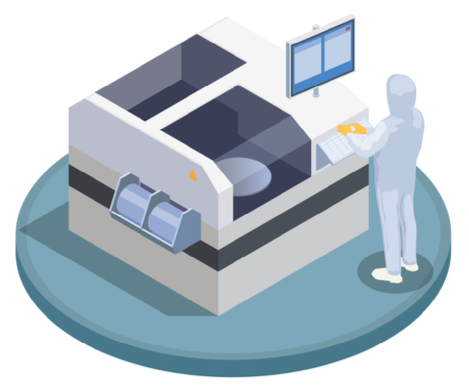 The R&D process of ASIC requires tape-out. For a 14nm process, tape-out costs around $3 million. For a 5nm process, it can be as high as $47.25 million.If tape-out fails, all the money is wasted, along with a significant amount of time and effort. Generally, small companies cannot afford this.So, does this mean that small companies cannot engage in chip customization?Of course not. Next, we will introduce another amazing tool—FPGA.█ FPGA (Field Programmable Gate Array)FPGA, short for Field Programmable Gate Array, has been very popular in the industry in recent years, even more so than ASIC, and is often referred to as a “universal chip”.In simple terms, FPGA is a reconfigurable chip. It can be repeatedly programmed an unlimited number of times after manufacturing to achieve desired digital logic functions based on user needs.The reason FPGA can achieve DIY is due to its unique architecture.FPGA consists of three types of programmable circuits: Configurable Logic Blocks (CLB), Input/Output Blocks (IOB), and Programmable Interconnect Resources (PIR), along with static memory SRAM.
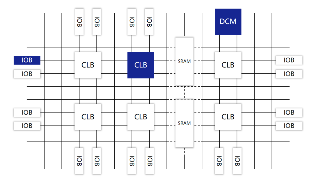 CLB is the most important part of FPGA, serving as the basic unit for implementing logic functions and carrying the main circuit functions.They are usually arranged in a regular array (Logic Cell Array, LCA) scattered throughout the chip.IOB mainly completes the interface between logic on the chip and external pins, typically arranged around the chip.PIR provides ample wiring resources, including horizontal and vertical mesh wiring, programmable switch matrices, and programmable connection points. They serve to connect and form circuits with specific functions.Static memory SRAM is used to store programming data for internal IOB, CLB, and PIR, controlling them to complete system logic functions.CLB itself is primarily composed of Look-Up Tables (LUT), multiplexers, and flip-flops, which are used to carry individual logic “gates” in the circuit and can be used to implement complex logic functions.In simple terms, we can understand LUT as RAM that stores computation results. When the user describes a logic circuit, the software calculates all possible results and writes them into this RAM. Each signal performing a logic operation is equivalent to inputting an address to look up a table. LUT will find the content corresponding to the address and return the result.This “hardware-based” computation method clearly provides faster computation speed.When users use FPGA, they can complete circuit design through hardware description languages (Verilog or VHDL), then “program” (burn) the FPGA, loading the design onto the FPGA to achieve the corresponding functionality.When powered on, FPGA reads data from the EPROM (Erasable Programmable Read-Only Memory) into SRAM, and after configuration, the FPGA enters operational status. After power-off, the FPGA reverts to a blank state, and the internal logic relationships disappear. This cycle achieves “on-site” customization.FPGA’s functionality is incredibly powerful. Theoretically, if the scale of gates provided by FPGA is large enough, it can achieve any ASIC’s logic function through programming.
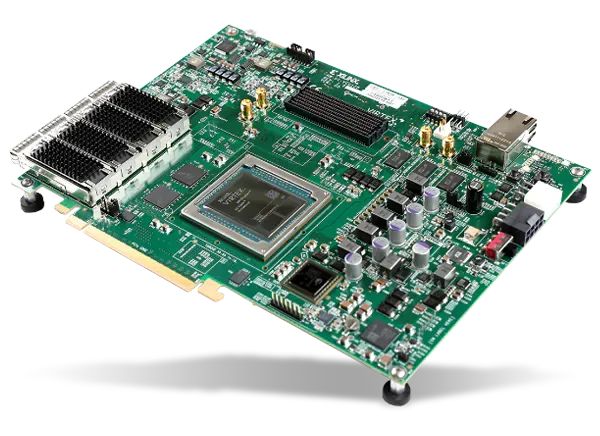 FPGA development kit, with the FPGA chip in the middleNow, let’s look at the development history of FPGA.FPGA developed from programmable devices like PAL (Programmable Array Logic) and GAL (Generic Array Logic), and belongs to a type of semi-custom circuit.It was invented in 1985 by Xilinx. Later, companies like Altera, Lattice, and Microsemi also entered the FPGA field, eventually forming a four-giant structure.In May 2015, Intel acquired Altera for a staggering $16.7 billion, later integrating it into the PSG (Programmable Solutions Group) department.In 2020, Intel’s competitor AMD also made a move, acquiring Xilinx for $35 billion.Thus, the four giants became Xilinx (under AMD), Intel, Lattice, and Microsemi (changing names but not the essence).In 2021, the market shares of these four companies were 51%, 29%, 7%, and 6%, respectively, totaling 93% of the global market share.Recently, in October 2023, Intel announced plans to split the PSG department for independent business operation.As for domestic FPGA manufacturers, they include Fudan Microelectronics, Unisoc, Anlu Technology, Dongtu Technology, Gaoyun Semiconductor, Jingwei Qili, Jingwei Yage, Zhiduojing, and Aoge Chip, among others. While the number seems considerable, the technical gap is significant.█ Differences Between ASIC and FPGANext, we will focus on the differences between ASIC and FPGA, as well as their differences from CPU and GPU.ASIC and FPGA are essentially chips. ASIC is a fully custom chip with fixed functions that cannot be changed, while FPGA is a semi-custom chip with flexible functions and high playability.We can illustrate the differences between the two through an example.ASIC is like using molds to make toys. It requires mold opening in advance, which is quite labor-intensive. Moreover, once the mold is opened, it cannot be modified. If new toys are to be made, a new mold must be opened.On the other hand, FPGA is like using LEGO bricks to build toys. You can start building right away, and after spending a little time, you can finish it. If you’re not satisfied or want to build a new toy, you can disassemble it and rebuild it.
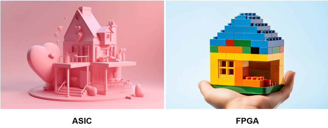 Many design tools for ASIC and FPGA are the same. In terms of design processes, FPGA is less complex than ASIC, omitting some manufacturing processes and additional design verification steps, approximately only 50%-70% of the ASIC process. The most cumbersome tape-out process is not required for FPGA.This means that developing ASIC may take several months or even over a year, while FPGA only requires several weeks or months.Earlier, we mentioned that FPGA does not require tape-out. Does this mean that FPGA costs are always lower than ASIC?Not necessarily.FPGA can be prefabricated and programmed in the lab or on-site without incurring non-recurring engineering (NRE) costs. However, as a “universal toy”, its cost is 10 times that of ASIC (molded toys).If production volume is relatively low, FPGA will be cheaper. If production volume is high, the one-time engineering costs of ASIC will be spread out, making ASIC cheaper.This is similar to mold opening costs. Opening molds is expensive, but if sales are high, it becomes cost-effective.As shown in the figure below, 400,000 pieces serve as a boundary for the cost of ASIC and FPGA. For quantities below 400,000, FPGA is cheaper. Above 400,000, ASIC is cheaper.
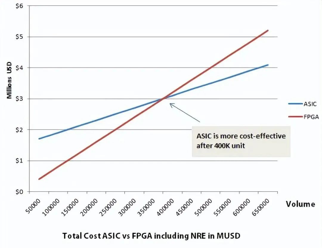 In terms of performance and power consumption, as dedicated custom chips, ASICs are stronger than FPGAs.FPGAs are general-purpose editable chips with more redundant functions. Regardless of your design, there will be some excess components.As mentioned earlier, ASIC is closely tailored, with little waste, and uses hard wiring. Therefore, it has stronger performance and lower power consumption.FPGA and ASIC are not simply competitive or substitutive; they have different positioning.FPGA is currently widely used for product prototype development, design iteration, and specific applications with low production volumes. It is suitable for products that require short development cycles. FPGA is also often used for ASIC verification.ASIC is used for designing large-scale, high-complexity chips, or for mature products with relatively high production volumes.FPGA is particularly suitable for beginners to learn and participate in competitions. Many university electronic programs now use FPGA for teaching.From a commercialization perspective, the main application fields of FPGA are communications, defense, aerospace, data centers, medical, automotive, and consumer electronics.FPGA has been used in the communications field for a long time. Many base station processing chips (baseband processing, beamforming, antenna transceivers, etc.) are made with FPGA. Core network coding and protocol acceleration also use it. Data centers previously utilized it in components like DPU.Later, as many technologies matured and stabilized, communication equipment manufacturers began to replace FPGA with ASIC to reduce costs.It is worth mentioning that in recent years, the popular Open RAN often uses general-purpose processors (Intel CPU) for computation. This solution’s energy consumption is far inferior to that of FPGA and ASIC. This is one of the main reasons why equipment manufacturers, including Huawei, are reluctant to follow Open RAN.In the automotive and industrial sectors, FPGA’s latency advantage is primarily why it is used in ADAS (Advanced Driver Assistance Systems) and servo motor drives.FPGA is used in consumer electronics because product iterations are too rapid. The development cycle of ASIC is too long; by the time something is made, it is already outdated.█ Which Is the Most Suitable AI Chip: FPGA, ASIC, or GPU?Finally, let’s return to the topic of AI chips.In the previous issue, Xiaozhao dropped a hint that AI computation divides into training and inference. Training is dominated by GPUs, while inference is not. I did not explain the reason.Now, I will explain.First, remember that purely from a theoretical and architectural perspective, the performance and cost of ASIC and FPGA are definitely superior to CPU and GPU.
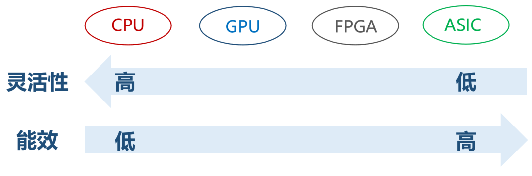 CPU and GPU follow the von Neumann architecture, where instructions go through storage, decoding, execution, etc., and shared memory undergoes arbitration and caching during use.FPGA and ASIC, however, are not based on the von Neumann architecture (they use Harvard architecture). For FPGA, its logical unit functions are determined during programming, representing hardware implementing software algorithms. For state retention needs, registers and on-chip memory (BRAM) in FPGA belong to their respective control logic, eliminating the need for arbitration and caching.In terms of the proportion of ALU operation units, GPUs have a higher ratio than CPUs, while FPGAs, with almost no control modules, have an even higher ratio of ALU operation units than GPUs.Therefore, comprehensively, FPGA’s computation speed is faster than that of GPUs.Now let’s discuss power consumption.GPUs are notoriously high in power consumption, with a single chip reaching 250W or even 450W (RTX4090). In contrast, FPGA typically only consumes 30 to 50W.This is mainly due to memory reading. The memory interface of GPUs (GDDR5, HBM, HBM2) has extremely high bandwidth, about 4-5 times that of FPGA’s traditional DDR interface. However, in terms of the chip itself, the energy consumed by reading DRAM is over 100 times that of SRAM. The frequent reading of DRAM by GPUs leads to extremely high power consumption.Additionally, FPGA’s operating frequency (below 500MHz) is lower than that of CPUs and GPUs (1-3GHz), contributing to lower power consumption. FPGA’s lower operating frequency is mainly limited by wiring resources. Some wires need to be routed far, and if the clock frequency is too high, it won’t be able to keep up.Finally, let’s look at latency.GPUs have higher latency than FPGAs.GPUs typically need to divide different training samples into fixed-size “batches” to maximize parallelism, requiring multiple batches to be gathered together for unified processing.FPGA’s architecture is batch-less. After processing a data packet, it can output immediately, giving it an advantage in latency.So, the question arises. If GPUs are inferior to FPGAs and ASICs in many aspects, why have they become so popular in AI computation?It’s simple: in the extreme pursuit of computing power performance and scale, the entire industry currently does not care about cost and power consumption.With NVIDIA’s long-term efforts, the core count and operating frequency of GPUs have been continuously improved, and the chip area has been increasing, focusing on brute-force computing power. Power consumption relies on process technology and passive cooling, so as long as it doesn’t catch fire, it’s acceptable.In addition to hardware, in the previous article, Xiaozhao also mentioned that NVIDIA is very good at laying out software and ecosystems.The CUDA they developed is a core competitive advantage of GPUs. Based on CUDA, beginners can quickly get started with GPU development. They have cultivated a strong user base over the years.In contrast, FPGA and ASIC development is still too complicated and not suitable for widespread use.In terms of interfaces, although GPUs have a more singular interface (mainly PCIe) and are not as flexible as FPGA (FPGA’s programmability allows it to easily interface with any standard and non-standard interfaces), it is sufficient for servers; just plug it in and use it.Beyond FPGA, the reason ASIC cannot compete with GPUs in AI is largely due to its high costs, long development cycles, and significant development risks. The rapid changes in AI algorithms make the ASIC development cycle critical.For the above reasons, GPUs currently enjoy a favorable position.In AI training, GPUs have strong computing power, significantly improving efficiency.In AI inference, inputs are usually single objects (images), so the requirements are lower, and there is no need for much parallelism, making the GPU’s computing power advantage less pronounced. Many companies will start using cheaper, more energy-efficient FPGAs or ASICs for computation.Other computing scenarios are similar. For those who prioritize absolute computing performance, GPUs are the first choice. For those with lower computing performance requirements, FPGAs or ASICs can be considered to save costs.█ Final WordsThis concludes the introduction to the knowledge of CPU, GPU, FPGA, and ASIC.They are typical representatives of computing chips. Currently, all computing power scenarios are primarily handled by them.With the development of the times, computing chips are also showing new trends. For example, different computing chips are mixed and matched to leverage each other’s advantages. We call this method heterogeneous computing. Additionally, there are brain-like chips led by IBM, which simulate the processing of the human brain’s neural synapses and have also made breakthroughs and gained popularity. I will introduce this to you in the future if I have the opportunity.I hope Xiaozhao’s series of articles on chips will be helpful to everyone. If you like it, please follow, share, and like.Thank you!—— The End ——References:1. “Understanding the Concept and Working Principle of GPU”, Open Source LINUX;2. “Overview of AI Chip Architecture”, Zhihu, Garvin Li;3. “What Are the Differences Between GPU, FPGA, and ASIC Accelerators?”, Zhihu, Hu Shuo Mantan;4. “Deep Dive into GPU, FPGA, and ASIC”, Automotive Industry Frontline Observation;5. “Why GPU Is the Core of Computing Power in the AI Era”, Muxi Integrated Circuit;6. “Overview of the Three Main Chip Architectures for Autonomous Driving”, Digital Transformation;7. “AIGC Computing Power Panorama and Trend Report”, Quantum Bit;8. Baidu Encyclopedia, Wikipedia.