This Citation Information (Click the title to read the full text)
DANG Haotian, LIU Dong, CHEN Fei, et al. Voltage control strategy for distribution network based on SoC FPGA hardware parallel computing[J]. Electric Power Engineering Technology, 2022, 41(3): 39-47, 91.
Abstract
With the development of active distribution networks and Internet of Things technology, the integration of reactive power devices has become complex and marginalized, leading to the evolution of voltage control calculations towards edge computing. Due to limited computing power, the time required for purely software-based calculations at edge terminals is lengthy and cannot meet the real-time requirements of control. To address this issue, this paper proposes a voltage control strategy for distribution networks based on System on Chip Field Programmable Gate Arrays (SoC FPGA) hardware parallel computing. First, a soft and hardware computing framework based on SoC FPGA is designed; then, targeted improvements are made to the distribution network voltage control model and genetic algorithm solving method suitable for FPGA computation; finally, the FPGA hardware solving structure is designed in modules. Validation through case scenarios shows that compared to the purely software-solving method at edge terminals, the proposed strategy improves the average solving efficiency by 2.41 times and 2.15 times in scenarios of voltage approaching the lower and upper limits, respectively, effectively enhancing the real-time performance of voltage control.
Voltage Control Technology Based on SoC FPGA Hardware Parallel Computing
DANG Haotian1, LIU Dong1, CHEN Fei1, ZHAO Xianping2, LIU Siyang2, WANG Hongyu3
1. School of Electronic Information and Electrical Engineering, Shanghai Jiao Tong University; 2. Yunnan Power Grid Co., Ltd; 3. Jiangsu Jinzhit Technology Co., Ltd.
Introduction
The issue of voltage exceeding limits is a key problem affecting the power quality of distribution networks. In the context of low carbon, an increasing number of distributed generators (DG) are connected to the distribution network. Compared to traditional distribution networks, the voltage of distribution networks with high DG penetration rates exhibits greater volatility, which places higher demands on the real-time control of distribution network voltages. The IEEE 1547 standard has set clear limitations on the duration of voltage exceeding limits.
DG itself is also a type of adjustable resource. How to fully utilize adjustable devices, including DG, is key to voltage regulation in distribution networks. However, different adjustable devices have different electrical characteristics, and the collaborative handling of different devices greatly increases the computational complexity of voltage regulation. Moreover, as the number of adjustable devices increases, the number of variables to be solved for voltage regulation also increases, leading to a significant increase in solving time for traditional centralized computing methods, which contradicts the real-time requirements of voltage control. Therefore, voltage control is evolving towards edge computing, where calculations are performed on adjustable devices in the vicinity of the edge nodes, reducing both the number of variables to be solved and the network transmission delay.
Currently, voltage control methods for distribution networks containing various DGs are mainly divided into two categories. The first category is voltage zoning control. This method generally uses corresponding rules to partition system nodes into regions; if the voltage at a certain node exceeds the limit, the adjustable devices within the region adjust their output to restore the voltage to normal, generally applicable to larger-scale distribution networks with sufficient reactive power devices. The basis for zoning is a research focus, with different literature proposing various zoning bases for different scenarios, achieving favorable application results. On the basis of zoning, other literature has proposed a hierarchical concept. Literature has divided the control area into autonomous control areas and coordinated control areas, with the voltage exceeding limit problem being solved collaboratively by the autonomous and coordinated control areas. Although the hierarchical zoning control strategy has advantages such as no need for iterative calculations and rapid response, its calculations are only targeted at a specific area, neglecting or giving less consideration to the connections with other areas, thus failing to achieve a global optimal solution. The second category of voltage control methods directly solves the reactive optimization problem, which is a control method based on optimization theory, generally applicable to smaller-scale and simpler distribution networks. Many studies have directly solved this using heuristic algorithms, and other studies have used second-order cone relaxation methods to convexify the original non-convex optimization model. Literature has proposed a reactive optimization method based on equivalent single-phase distribution networks using second-order cone relaxation transformations. Literature has proposed a second-order cone relaxation model suitable for reactive optimization of three-phase unbalanced active distribution networks. Additionally, literature has linearized the flow equations when solving non-convex nonlinear reactive optimization problems. Although the above methods can obtain approximately globally optimal solutions, they are computationally complex at the software level, and coupled with insufficient computing power at edge terminals, they cannot meet the real-time requirements of voltage control.
In edge computing, the core of simultaneously satisfying the global nature and real-time nature of regional solving lies in improving the computing power of edge terminals. However, limited by cost, the configuration of central processing units (CPUs) and memory resources at terminals cannot reach the level of central servers, and the efficiency of purely software calculations is limited. In addition, many edge computing studies focus on utilizing hardware-assisted computing, such as using field-programmable gate arrays (FPGAs) to assist CPU calculations. FPGAs are suitable for parallel computing, and their advantages in parallel computation have been validated in applications such as waveform recording systems, neural networks, and video detection and tracking.
System on Chip Field Programmable Gate Arrays (SoC FPGAs) can be considered a combination of CPUs and FPGAs, which can fully utilize the parallel computing advantages of FPGAs and the general computing capabilities of CPUs in calculations, effectively improving computing efficiency. Considering the voltage control in edge computing scenarios, this paper proposes a voltage control strategy based on SoC FPGAs. To balance the global and efficient nature of control, a simplified reactive optimization model is proposed, and an improved parallel genetic algorithm suitable for FPGA computation is designed and implemented, providing an effective solution for enhancing the speed of voltage control on the edge side.
1. Voltage Control Model and Algorithm Suitable for FPGA Computation
Unlike centralized control, the voltage control strategy in this paper is oriented towards the edge side, with the control object being the voltage of all nodes on a feeder line, and the control method being local control after computation at the edge terminal. Although a feeder line is only part of the distribution network, it can be seen as a small distribution network, and the reactive control model and algorithm for the distribution network can also be applied to a single feeder line.
1.1
Simplified Voltage Control Model Suitable for FPGA Computation
The topology of the terminal cascaded hybrid DC transmission system is shown in Figure 1.
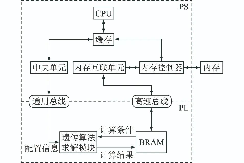
Figure 1 SoC FPGA Data Processing Architecture
The rectifier station is composed of two sets of 12-pulse LCCs in series, while the inverter station is composed of one set of 12-pulse LCCs and a series of MMCs in parallel, with the MMC parallel group consisting of three half-bridge MMCs in parallel. The rated voltage and active power of the hybrid DC system are 800 kV and 4,000 MW, respectively, with the rated voltage and active power of the high-end LCC on the inverter side being 400 kV and 2,000 MW, and the rated voltage and active power of the three MMC converters at the low end being 400 kV and 667 MW, respectively. On the other hand, the inverter stations at the receiving end feed into different locations of the 500 kV AC system.
Voltage control can be regarded as a reactive optimization problem in power systems. When the voltage at a certain node in the system exceeds the limit, the reactive devices in the system, such as energy storage devices, capacitor banks, and DGs, can be adjusted to regulate the reactive distribution in the system and thus adjust the node voltage.
The objective function of reactive optimization is generally to minimize the voltage deviation of system nodes or the system network loss. This paper takes the minimization of the voltage deviation of system nodes as the objective function. The constraints include equality constraints and inequality constraints. The equality constraints are flow balance constraints.
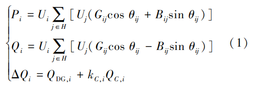
Where: Pi, Qi are the injected active power and reactive power at node i; Ui, Uj are the voltages at nodes i and j; Gij, Bij, θij are the conductance, susceptance, and voltage phase angle difference between nodes i and j, respectively; H is the set of node numbers in the system; ΔQi is the output of adjustable reactive devices at node i; QDG, i is the output of DG at node i; kC, i, QC, i are the number of capacitor banks turned on at node i and the output of a single capacitor bank, where kC, i is a non-negative integer.
The inequality constraints include node voltage constraints, node power constraints, and output constraints for DGs and capacitor banks.
The reactive optimization problem is to solve for a set of adjustable reactive device outputs that minimize the objective function value while satisfying the equality and inequality constraints. For this non-convex nonlinear optimization problem, even if the voltage control target is only one feeder line containing various DGs, it still requires a long computation time, thus necessitating appropriate simplifications of the solving model and parallel designs of the algorithm.
The flow balance calculation shown in Equation (1) requires multiple iterations. If FPGA is used for iterative calculations, a large number of input and output operations are required. Moreover, this calculation process involves a large number of trigonometric functions and complex number computations, requiring significant FPGA computational resources, which will greatly increase computation time. This paper focuses on the influence of DG output on voltage magnitude, and when the output changes slightly, the Jacobian matrix in the flow calculation can be approximated as constant. Within the allowable precision range for engineering operations, this approximation can greatly enhance the real-time performance of voltage control.
Approximate power balance can be represented by the voltage sensitivity matrix. The voltage sensitivity matrix reflects the unit power change at a certain node’s impact on the voltages of all nodes in the system and can be derived from the flow balance equations. Based on real-time electrical data streams and system network parameters, we have:

Where: P, Q are the injected active and reactive powers at each node; V, δ are the voltage magnitudes and angles at each node; S is the voltage sensitivity submatrix.
This paper uses adjustable reactive devices to adjust reactive output, thereby adjusting voltage, assuming ΔP=0. Therefore, the voltage sensitivity matrix is:

S reflects the sensitivity of the node voltage change to the change in reactive power. S is a constant matrix, and the influence of changes in a certain node’s reactive power on the voltages of all nodes can be directly approximated using S. The flow constraints in Equation (1) can be simplified to:

That is:
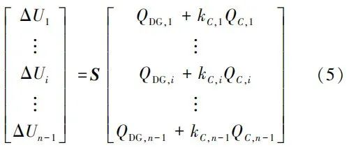
Where: n is the number of nodes.
The reactive optimization problem is thus to solve for the reactive outputs in Equation (5). In Equation (5), QC, i is a known quantity, so the reactive optimization problem can be transformed into solving [QDG, 1 kC, 1 … QDG, i kC, i … QDG, n-1 kC, n-1]T.
1.2
Improved Parallel Genetic Algorithm Suitable for FPGA Computation
For the above reactive optimization problem, traditional solving algorithms include voltage zoning control algorithms and heuristic optimization algorithms. The former obtains local solutions, while the latter obtains global solutions. This paper combines these two algorithms to propose an improved parallel genetic algorithm suitable for rapid solving on FPGA.
1.2.1 Traditional Reactive Optimization Solving Algorithm
In voltage zoning control, a critical value ΔUth is first defined. For the unit injection of reactive power by the reactive power source, if the voltage change at a certain node exceeds ΔUth, this node is included in the voltage control domain of that reactive power source. When the voltage at a certain node exceeds the limit, only the reactive power sources within the voltage control domain of that node need to be adjusted. The voltage zoning control method has advantages such as speed and no need for multiple iterative calculations, but it neglects the role of reactive power sources outside the control domain, thus only providing a rough local solution and failing to achieve a global optimal solution.
To obtain the global optimal solution for the reactive optimization problem, heuristic algorithms such as particle swarm optimization, harmony search, and genetic algorithms are generally used to search for global or approximate global optimal solutions. Genetic algorithms are chosen for their fast convergence speed and suitability for parallel computing; this paper introduces the genetic algorithm as an example, which will be implemented on FPGA to solve the reactive optimization problem.
The classic steps of the genetic algorithm for voltage control problems are: (1) Generate the initial population, where each individual represents a reactive output vector; (2) Enter the iterative calculation process, performing selection, crossover, and mutation operations while ensuring that the newly generated individuals meet power requirements; (3) Calculate the fitness, substituting the newly generated individuals into Equation (5) to compute the objective function value (fitness value in the genetic algorithm) and store it; (4) After one generation of evolution, if the solving requirements are not met, return to step (2) and repeat the iterative process.
Although genetic algorithms can compute solutions close to the global optimal solution, the iterative processes can affect computational efficiency.
1.2.2 Improved Parallel Genetic Algorithm
Considering that the genetic algorithm’s encoding and solving methods are inherently parallel, suitable for FPGA acceleration, the main solving body for the reactive optimization problem is selected as the genetic algorithm. Additionally, to simultaneously meet global and real-time requirements, improvements to the genetic algorithm are proposed as follows.
(1) The population initialization process introduces the voltage zoning control strategy. Since the selection of the initial population in the genetic algorithm significantly impacts the convergence and efficiency of the algorithm, a completely random initial population may lead to poor convergence. Considering the characteristics of the impact of the distribution network’s reactive output on voltage, the theoretical global optimal solution is close to the local optimal solution generated by the voltage zoning control algorithm. Therefore, to improve convergence speed, part of the initial population is set as individuals directly derived from the voltage zoning control, while the rest are generated randomly.
(2) In the iterative calculation process, population-level and gene-level parallel solving is applied. Population-level parallelism divides a large population into multiple smaller populations, which perform genetic calculations in parallel, only communicating between populations after a certain number of generations. Gene-level parallelism refers to simultaneous operations on different loci of the same vector, which are widely applied in selection, crossover, mutation, and fitness calculation operations during the iterative process. Unlike the serial execution characteristics of CPUs, FPGAs are specialized hardware circuits, and both population-level and gene-level parallelism can be achieved by increasing hardware resources.
(3) The iterative calculation process is pipelined. The selection, crossover, mutation, and fitness calculation operations in the genetic algorithm sequentially form an execution cycle. In FPGA design, different operations correspond to different hardware modules; adopting a pipelined calculation method can effectively reduce module idle rates and enhance computational efficiency.
2. Voltage Control Processing Flow Based on SoC FPGA
2.1
SoC FPGA Processing Platform
The complete voltage control flow requires collaborative computation between the CPU and FPGA. SoC FPGA provides a fully programmable SoC for embedded systems, combining general processors with programmable logic. The internal architecture of SoC FPGA can be divided into two parts: processing system (PS) and programmable logic (PL), which communicate through a high-speed interface. This architecture supports hardware logic design in the PL part while performing software design in the PS part.
2.2
Design of Voltage Control Processing Flow
The SoC FPGA serves as the computation and control center, and its data processing architecture is designed as shown in Figure 1. During processing, the PS side first receives real-time electrical signals from the distribution network through a Gigabit Ethernet port and performs flow calculations and S calculations, then updates the S calculation results in real-time to the block random access memory (BRAM) on the PL side via the advanced extensible interface (AXI). BRAM serves as a bridge for data interaction between the PS and PL sides.
Simultaneously, the PS side performs real-time calculations of S rather than waiting until voltage exceeding limits are detected, as the calculation of S is time-consuming. If calculations are performed only after detecting voltage exceeding limits, it would significantly increase the computation time for reactive optimization. Since S changes very little in a short time, during reactive optimization calculations, using the S from the previous time point can ensure calculation accuracy without incurring the time cost of recalculating. Here, the calculation cycle for S is set to 2 seconds. The PL side can directly access the S data from BRAM upon receiving the calculation instructions.
Once the PS side detects voltage exceeding limits, it immediately transmits the real-time node voltage data, voltage and power constraint conditions, and the generated partial initialization population to the fixed corresponding addresses in BRAM via AXI, triggering the parallel computation module on the PL side to perform reactive optimization calculations based on the genetic algorithm. After the PL side completes the calculations, it transmits the final results back to the PS side via interrupts. The PS side then decides whether to issue reactive adjustment instructions or report the results to the central cloud server. The workflow of the collaborative computation between the PS and PL sides is illustrated in Figure 2.
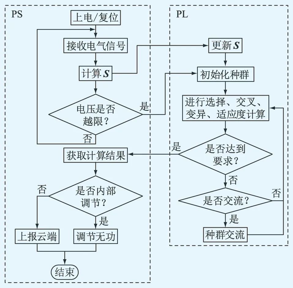
Figure 2 Collaboration Workflow Between PS and PL Sides
3. Design of Parallel Genetic Algorithm Suitable for FPGA Computation
In the design, S is calculated in real-time and does not block the solving process, hence the main factor affecting the solving time for reactive optimization is the efficiency of the genetic algorithm. This paper designs an improved genetic algorithm for voltage control solving, applied in modules on FPGA.
3.1
Hardware Architecture Design
Hardware design on FPGA typically adopts a top-down modular design approach. Each step of the genetic algorithm is designed as a separate hardware module, connected according to the data flow logic. The PL side modular system structure design is shown in Figure 3.
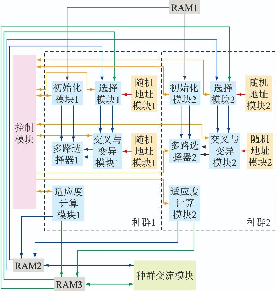
Figure 3 Parallel Genetic Algorithm System Structure (Parallelism Level 2)
3.2
Encoding Design
The system’s adjustable reactive devices include DGs and capacitor banks at each node. The former are continuous variables, while the latter are discrete variables. For nodes containing DGs or capacitor banks, an 11-bit encoding is used to represent the output of the DG at that node, with the first bit as the sign bit corresponding to an adjustable range of -1,024 to 1,024 kvar; a 5-bit encoding is used to represent the number of capacitor banks turned on, with the first bit also as the sign bit corresponding to an adjustable range of -16 to 16 banks. These changes cover the value ranges for the output of node DGs or the number of capacitor banks turned on. The variable encoding for a single node is shown in Figure 4.

Figure 4 Encoding Format for a Single Node
Assuming there are T nodes in the distribution network with reactive regulation capabilities, each individual in the genetic algorithm population can be represented as a string of 16T numbers connected, i.e., [QDG, 1 kC, 1 … QDG, i kC, i … QDG, T kC, T]T, with a total encoding length of 16T.
3.3
Key Points of Modular Hardware Design
There are detailed descriptions in the literature regarding the genetic algorithm based on software solving; this section focuses on the differences in FPGA solving compared to software solving and the adaptive improvements for voltage regulation scenarios.
(1) A control module is designed to ensure the orderly and normal operation of the hardware system. Unlike the inherent serialization processing in CPUs, the serialization of different modules in FPGA requires the support of a finite state machine. The control module implements signal interactions with other modules through a finite state machine suitable for the genetic algorithm.
The evolution process of each population is divided into seven states. The idle and stop states represent reset and termination signals, respectively. The other five states are working states, namely population initialization, selection state, crossover mutation, fitness calculation, and population communication. The state transitions are shown in Figure 5.
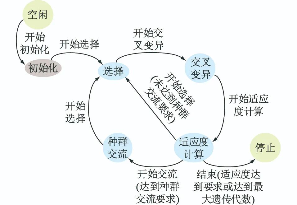
Figure 5 Control Module Finite State Machine
(2) The initialization module design incorporates the voltage zoning control idea to improve the convergence speed of the genetic algorithm. The selection of the initial population significantly impacts the convergence of the genetic algorithm. The reactive adjustment solutions provided by the zoning control strategy are relatively rough, but given practical circumstances, this solution is close to the final global optimal solution; thus, it can be used as part of the initial population to enhance algorithm convergence speed.
In this paper, 25% of the individuals in the initial population are derived from the voltage zoning control strategy, while the remaining 75% are randomly generated. This setup utilizes the results from the zoning control algorithm to improve convergence speed while preventing the algorithm from falling into premature or local optimal solutions.
(3) Since FPGAs are not well-suited for probabilistic calculations, a new selection mechanism must be designed. The implementation of this mechanism requires the cooperation of the selection module, storage module, and random number generation module.
The commonly used selection operations include roulette wheel selection and random tournament selection. The core idea of roulette wheel selection is to give more excellent individuals a higher probability of being selected, with the probability of each individual being selected being the ratio of its fitness to the sum of the fitness of all individuals in the population. Random tournament selection is simpler, randomly selecting an even number of individuals from the population to compare in pairs, with the more excellent individuals retained.
Although roulette wheel selection is more reasonable, due to the complexity of handling decimals and probabilities in FPGA, the selection mechanism designed in this paper is based on random tournament selection while incorporating the idea of proportional selection. This mechanism relies on the setup of the storage module, which stores two new individuals and their corresponding fitness values each time, comparing the fitness values before storage; the higher fitness individual is stored in the upper half of the population, while the lower fitness individual is stored in the lower half.
The positions of the randomly selected individuals in the selection operation are generated by the random number module, and by modifying the random numbers, individuals in the upper half of the population have a higher probability of being selected, thus approaching the results of roulette wheel selection. The random number generation module is an x-bit linear feedback shift register, as shown in Figure 6.

Figure 6 Random Number Generation Module
(4) The hardware circuits are duplicated to achieve parallel evolution of the population, and a population communication module is designed to facilitate communication between populations. The parallel evolution of populations can improve the parallelism of the genetic algorithm’s computations and independently develop different excellent gene segments. Meanwhile, population communication helps concentrate excellent genes, evolving more outstanding individuals. In the design, population communication is represented as the replacement of the worst individual in one population with the best individual in another population. Assuming the parallelism level of population evolution is m, the communication process between populations is shown in Figure 7.
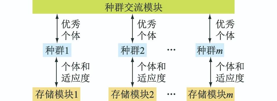
Figure 7 Schematic of Population Communication Process
(5) The internal multiply-add calculations and matrix calculations within each module are achieved through increased hardware resources, enabling gene-level parallelism. Crossover and mutation operations employ multi-point crossover and multi-point mutation. For multi-point operations, hardware units can be duplicated in FPGA to achieve parallel operations.
The fitness calculation module is the most resource-intensive module and the one that can significantly enhance computational efficiency through FPGA parallel computing. Since the outputs of the individuals from the crossover mutation module already meet power constraint conditions, only the voltage exceeding limit problem is considered during fitness calculations. In this paper, the consideration of voltage constraint issues is reflected in the segmented design of the penalty factor for the objective function. When a node’s voltage exceeds the limit as computed by S, the penalty factor for that node’s corresponding term is greater than for other non-exceeding terms, and the greater the voltage deviation, the larger the penalty factor, leading to a higher final objective function value. After several generations of selection, it is evident that individuals with voltage exceeding limits will have their gene segments eliminated.
Based on the above analysis, the fitness calculation module only needs to compute the objective function value corresponding to the input individuals without considering constraint conditions. The calculation of the objective function value involves matrix operations and multiple multiply-add operations, allowing for full utilization of FPGA’s parallel computing capabilities.
The steps for fitness calculation are: mapping the number of capacitor banks to reactive output and summing it with DG output to form the reactive output vector; substituting it into Equation (5) for calculations, obtaining the voltage increments at each node, and substituting them into the objective function to calculate fitness.
All multiply-add calculations and matrix calculations in the above steps can be solved in parallel by stacking hardware resources.
4. Case Analysis
4.1
Parameter Settings
This paper analyzes a case derived from a certain distribution system. The case includes 62 nodes and a total of 3 feeders, which are interconnected by tie lines. This paper focuses on voltage control for a single feeder on the edge side, not involving reactive support between feeders, hence one feeder is selected for detailed analysis, with its topology shown in Figure 8. The system base voltage is 10 kV, the base capacity is 10 MW, and the acceptable voltage deviation range for each node is -0.05 to 0.05 p.u., with loads treated as constant power loads. To validate the voltage control strategy proposed in this paper, the following modifications are made to the case: DGs are installed at nodes 3, 5, and 11, with each DG’s reactive output range being 0 to 600 kvar, each DG’s capacity being 1 MV·A, and each inverter’s capacity being 1.2 MV·A. At nodes 2 and 9, 10 capacitor banks are installed, with each capacitor bank’s capacity being 25 kvar.
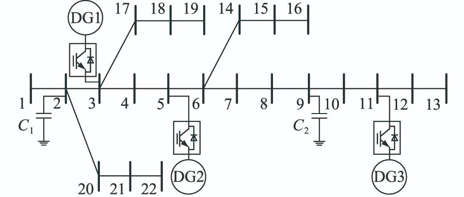
Figure 8 Feeder Topology
The case derived from a certain distribution system contains 62 nodes and a total of 3 feeders, interconnected by tie lines. This paper focuses on voltage control for a single feeder on the edge side, not involving reactive support between feeders, hence one feeder is selected for detailed analysis, with its topology shown in Figure 8. The system base voltage is 10 kV, the base capacity is 10 MW, and the acceptable voltage deviation range for each node is -0.05 to 0.05 p.u., with loads treated as constant power loads. To validate the voltage control strategy proposed in this paper, the following modifications are made to the case: DGs are installed at nodes 3, 5, and 11, with each DG’s reactive output range being 0 to 600 kvar, each DG’s capacity being 1 MV·A, and each inverter’s capacity being 1.2 MV·A. At nodes 2 and 9, 10 capacitor banks are installed, with each capacitor bank’s capacity being 25 kvar.
Set ΔUth to 0.08 p.u. When the voltage change at a certain node reaches the threshold of multiple adjustable devices simultaneously, it will be assigned to the adjustable device that causes the largest voltage change. Based on this, the system is divided into two voltage control domains, as shown in Table 1.
The individual generation strategy is set as follows: select the node with the most severe voltage exceeding limit, primarily adjusting the reactive output of the adjustable reactive devices in that node’s control domain, with the output of reactive devices outside the control domain adjusted as secondary. The total amount of reactive output adjustment is set as a constant value ΔQch, which is the increase or decrease in reactive value required to raise the voltage at that node to 1.02 p.u. or lower it to 0.98 p.u. ΔQch consists of reactive outputs from both within and outside the control domain. The output ratios of adjustable devices within the control domain are set to 0.95ΔQch, 0.90ΔQch, 0.85ΔQch, 0.80ΔQch, ensuring that the output within the domain is dominant. In specific allocations, the output distribution within the control domain is weighted according to the voltage sensitivity coefficients of the nodes where different adjustable devices are located, while the output of reactive devices outside the control domain is randomly allocated.
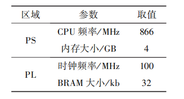
The parameters for the genetic algorithm using FPGA hardware parallel computing are set as shown in Table 2. The hardware parameters of the SoC FPGA are shown in Table 3.
Table 1 Voltage Control Domain Division
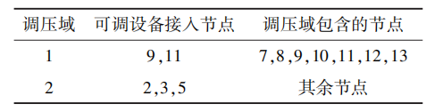
Table 2 Parallel Genetic Algorithm Parameter Settings
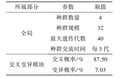
Table 3 Hardware Parameters of SoC FPGA
4.2
Simulation Verification and Analysis
4.2.1 Initial System State
The design aims to balance the global accuracy of voltage control on the edge side with high computational efficiency. Two scenarios of node voltage exceeding lower and upper limits are analyzed, with the initial voltages for both scenarios shown in the initial voltage figures 9 and 10.
Let the voltage control method combining SoC FPGA hardware and software be referred to as Method I. The following three solving methods are compared with Method I.
Method II: Voltage zoning control method. The reactive adjustment amount of adjustable devices is directly given by the voltage zoning control strategy.
Method III: Pure software non-iterative method. The FPGA parallel genetic algorithm solving part is replaced with software computation, while other settings remain unchanged.
Method IV: Pure software iterative method. Based on Method III, the flow balance constraints of the original model are used in place of the voltage sensitivity matrix constraints in Equation (5). At this point, each fitness calculation completes a full flow calculation.
All four methods share the same initial population.
4.2.2 Global Accuracy
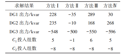
Applying the above four methods, the voltage adjustment effects and solving results for the voltage exceeding lower limit scenario are shown in Figure 9 and Table 4, while the voltage adjustment effects and solving results for the voltage exceeding upper limit scenario are shown in Figure 10 and Table 5.
Both scenarios’ solving results meet power constraints. Methods I and III employ simplified models for solving, while Method II uses the voltage zoning control method. From Figures 9 and 10, it can be seen that the voltages at the exceeding limit nodes in both scenarios can be restored to normal ranges, but for the voltage adjustments of other non-exceeding nodes (e.g., node 16) that are farther from the exceeding limit nodes, Method I significantly outperforms Method II. Therefore, compared to Method II, Method I exhibits better globality.
Method IV uses the original model for solving, and its results are compared with those obtained from the simplified model. Compared to the original model, the simplified model linearizes the flow balance conditions for computational efficiency, which may introduce some deviation when substituting the final approximate calculation results back into the actual flow calculations. However, considering the real-time nature of voltage adjustments, the significant improvement in computational efficiency outweighs the relatively small deviations caused by this approximate calculation.
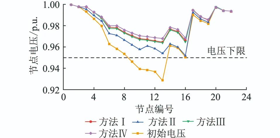
Figure 9 Comparison of Voltage Adjustment Effects in the Voltage Exceeding Lower Limit Scenario
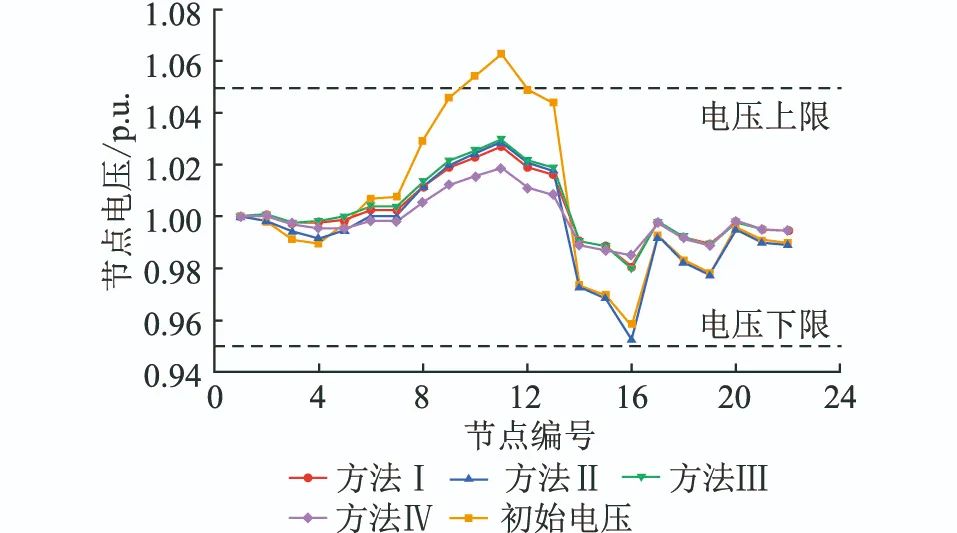
Figure 10 Comparison of Voltage Adjustment Effects in the Voltage Exceeding Upper Limit Scenario
Table 4 Solving Results of the Four Methods in the Voltage Exceeding Lower Limit Scenario
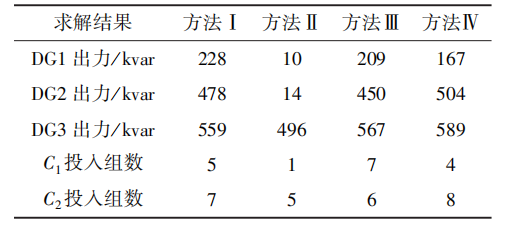
Table 5 Solving Results of the Four Methods in the Voltage Exceeding Upper Limit Scenario
4.2.3 Computational Efficiency
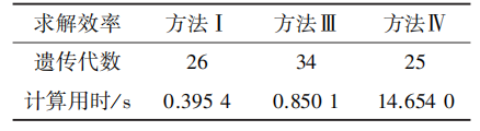
On the basis of ensuring global accuracy in control, the computational efficiency advantages of Method I are verified. The solving efficiency of Method I is compared with Methods III and IV, and after 10 random repetitions, the average solving time and genetic generations for the three methods are statistically analyzed. The solving efficiency comparisons for the two scenarios are shown in Tables 6 and 7.
From the analysis of Tables 6 and 7, it can be seen that the solving time of Method IV is significantly greater than that of Methods I and III. This is due to Method IV employing the original reactive control model, requiring complete flow calculations for each individual’s fitness in the genetic algorithm. Each flow calculation involves multiple iterations, greatly increasing computation time. Furthermore, the number of iterations in flow calculations is uncertain, leading to considerable variability in fitness calculation times. Therefore, Method IV lacks real-time capability, which also indicates the clear advantages of Method I in computational efficiency.
Furthermore, comparing Methods I and III shows that for the same computational load, Method I, utilizing FPGA-accelerated parallel computing for the genetic algorithm, has a significant time advantage over Method III’s pure software calculations. In the above two voltage exceeding scenarios, Method I’s computational efficiency improved by 2.41 times and 2.15 times compared to Method III, respectively. Finally, experiments indicate that in these two scenarios, the parallel acceleration ratios for Method I are 1.97 and 1.71, respectively.
In summary, in the above two voltage exceeding scenarios, the proposed method utilizing a simplified model and parallel genetic algorithm based on SoC FPGA can better balance the globality and efficiency of the solving process compared to other voltage control methods.
Table 6 Comparison of Solving Efficiency in the Voltage Exceeding Lower Limit Scenario
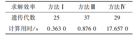
Table 7 Comparison of Solving Efficiency in the Voltage Exceeding Upper Limit Scenario
5. Conclusion
As more controllable DGs are integrated into distribution networks, traditional centralized voltage control computation methods have shown deficiencies in computational efficiency and control real-time performance; thus, voltage control in distribution networks is evolving towards edge computing. To achieve rapid voltage control at edge terminals, this paper proposes and implements a hardware parallel voltage control method based on SoC FPGA. This method combines voltage zoning control strategies and genetic algorithm solving methods, correctly delineating the responsibilities of software and hardware, computing the voltage sensitivity matrix non-blockingly on the software side, while leveraging the excellent parallel computing capabilities of FPGA on the hardware side to accelerate the solving of optimization problems. Comparative validation through case analysis shows that, compared to purely software-based computation methods, the proposed method can significantly enhance the real-time performance of voltage control.
In larger-scale distribution network systems with more DG connections, the parallelism of FPGA computing will correspondingly increase, thus further enhancing the computational efficiency of terminal devices. With the development of IoT and communication technology, the proposed method, due to its computational efficiency advantages, will have broad application prospects in the field of voltage control for distribution networks.
Key Authors and Team Introduction

DANG Haotian: Male, Master’s student, research direction in active distribution networks;
LIU Dong: Male, PhD, Professor, research direction in cyber-physical systems of power grids;
CHEN Fei: Male, PhD, research direction in active distribution networks.
↓ Related Articles ↓
DENG Zhenli, ZHANG Tao, LI Rong, et al. Active Distribution Network Active-Reactive Coordination Scheduling Method Based on ε-Relaxation[J]. Electric Power Engineering Technology, 2020, 39(4): 104-111.
ZHU Xiaojun, CHEN Xi, LI Yan, et al. Active Distribution Network Optimization Scheduling Considering Electric Vehicle Integration[J]. Electric Power Engineering Technology, 2021, 40(3): 141-147.
HE Tao, YIN Zhongdong, WANG Qunfei. Implementation Method of Hybrid Simulation Interface for Active Distribution Networks Based on Virtual Line Compensation[J]. Electric Power Engineering Technology, 2022, 41(3): 133-142.
Important Statement: According to the relevant regulations of the National Copyright Administration, reprinting or excerpting this WeChat article in paper media, websites, Weibo, and WeChat public accounts must include this WeChat name, QR code, and other key information, and indicate “Original by Electric Power Engineering Technology” at the beginning of the article. Individuals may forward and share according to this WeChat original text.
Editor: WANG Lulu
Review: JIANG Lin

 Click “Read the Original” to log in to the official website of Electric Power Engineering Technology.