1. Module Source>>>
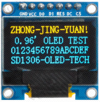
Module Physical Display:
Data Download Link: https://pan.baidu.com/s/1U9r32qeS2jOANB0SNwtwnw
Data Extraction Code: 8888
2. Specifications>>>
Refer to manufacturer documentation for the following information:
Operating Voltage: 3.3V
Operating Current: 15MA
Module Size: 27.3 x 27.8 MM
Pixel Size: 128(H) x 64(V) RGB
Driver Chip: SSD1306
Communication Protocol: SPI
Pin Count: 7 Pins (2.54mm pitch header)
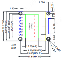
Size Parameters
Our goal is to port the example routine to the Lichuang CW32F030C8T6 development board. Follow the steps below to complete the porting.
-
Import the source code into the project;
-
Make rough modifications based on compilation errors;
-
Modify pin configurations;
-
Modify timing configurations;
-
Porting verification.
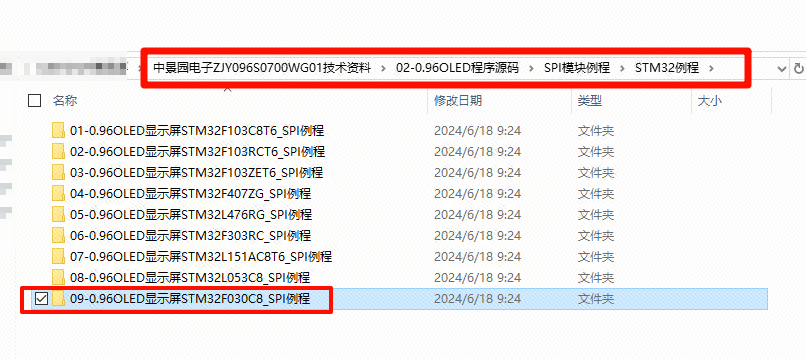
Open the manufacturer’s example documentation (example download link can be found in the cloud link). The specific path is shown in the image below.
3.2 Porting to Project
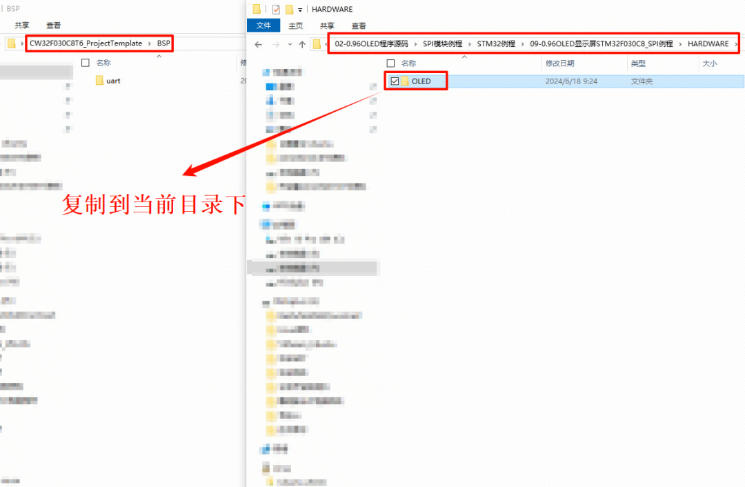
Copy the [OLED] folder from the manufacturer’s documentation path into your own project. Your project must have at least a millisecond delay function. (Refer to the introductory manual for the project)
Open your project and import the copied .c and .h files.
Then, in oled.h, add the following macro definition, changing sys.h to board.h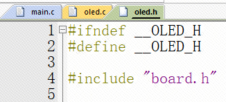
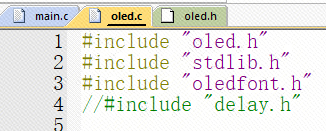
Next, comment out the #include “delay.h” in the oled.c file.
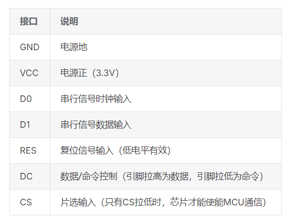
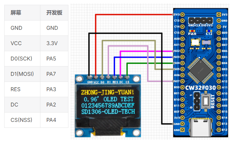
This screen requires the configuration of 7 interfaces; specific interface descriptions are shown in the table below.
The module operates as a slave in the SPI communication protocol, where D0 is the SPI signal line (SCK), D1 is the SPI output line (MOSI), and CS is the SPI chip select line (NSS). The following sections will explain both software SPI and hardware SPI porting.
3.3.1 Software SPI Porting
The current manufacturer’s source code uses a software SPI interface, and the SPI timing has already been completed by the manufacturer. We only need to configure the pins and delays accordingly. Therefore, please connect the screen pins as per your requirements. The selected pins are shown in the table below.
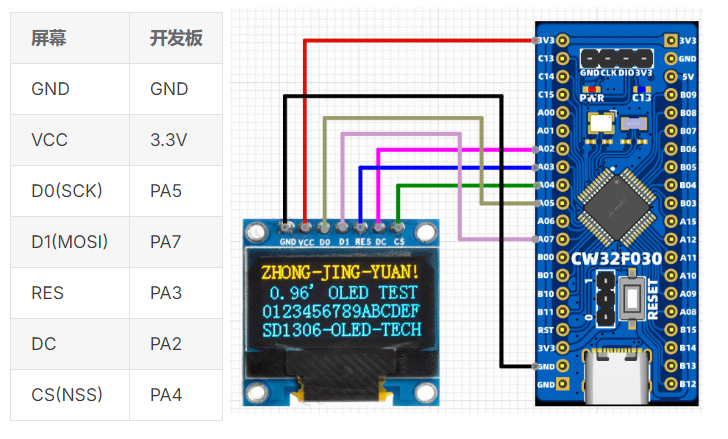
After selecting the pins, enter the project and start writing the screen pin initialization code. Modify the void OLED_Init(void) function in the oled.c source code as follows:
// OLED Initialization
void OLED_Init(void) {
GPIO_InitTypeDef GPIO_InitStruct; // GPIO initialization structure
__RCC_GPIOA_CLK_ENABLE(); // Enable GPIOA clock
GPIO_InitStruct.Pins = OLED_SCL_PIN| // GPIO pins
OLED_MOSI_PIN|
OLED_RES_PIN|
OLED_DC_PIN|
OLED_CS_PIN;
GPIO_InitStruct.Mode = GPIO_MODE_OUTPUT_PP; // Push-pull output
GPIO_InitStruct.Speed = GPIO_SPEED_HIGH; // High output speed
GPIO_Init(OLED_GPIO_PORT, &GPIO_InitStruct); // Initialize
OLED_RES_Clr();
delay_ms(200);
OLED_RES_Set();
OLED_WR_Byte(0xAE, OLED_CMD); // Turn off OLED panel
OLED_WR_Byte(0x00, OLED_CMD); // Set low column address
OLED_WR_Byte(0x10, OLED_CMD); // Set high column address
OLED_WR_Byte(0x40, OLED_CMD); // Set start line address (0x00~0x3F)
OLED_WR_Byte(0x81, OLED_CMD); // Set contrast control register
OLED_WR_Byte(0xCF, OLED_CMD); // Set SEG Output Current Brightness
OLED_WR_Byte(0xA1, OLED_CMD); // Set SEG/Column Mapping (0xa0 inverted, 0xa1 normal)
OLED_WR_Byte(0xC8, OLED_CMD); // Set COM/Row Scan Direction (0xc0 inverted, 0xc8 normal)
OLED_WR_Byte(0xA6, OLED_CMD); // Set normal display
OLED_WR_Byte(0xA8, OLED_CMD); // Set multiplex ratio (1 to 64)
OLED_WR_Byte(0x3f, OLED_CMD); // 1/64 duty
OLED_WR_Byte(0xD3, OLED_CMD); // Set display offset
OLED_WR_Byte(0x00, OLED_CMD); // No offset
OLED_WR_Byte(0xd5, OLED_CMD); // Set display clock divide ratio/oscillator frequency
OLED_WR_Byte(0x80, OLED_CMD); // Set divide ratio, Set Clock as 100 Frames/Sec
OLED_WR_Byte(0xD9, OLED_CMD); // Set pre-charge period
OLED_WR_Byte(0xF1, OLED_CMD); // Set Pre-Charge as 15 Clocks & Discharge as 1 Clock
OLED_WR_Byte(0xDA, OLED_CMD); // Set COM pins hardware configuration
OLED_WR_Byte(0x12, OLED_CMD);
OLED_WR_Byte(0xDB, OLED_CMD); // Set VCOMH
OLED_WR_Byte(0x40, OLED_CMD); // Set VCOM Deselect Level
OLED_WR_Byte(0x20, OLED_CMD); // Set Page Addressing Mode (0x00/0x01/0x02)
OLED_WR_Byte(0x02, OLED_CMD);
OLED_WR_Byte(0x8D, OLED_CMD); // Set Charge Pump enable/disable
OLED_WR_Byte(0x14, OLED_CMD); // Set (0x10) disable
OLED_WR_Byte(0xA4, OLED_CMD); // Disable Entire Display On (0xa4/0xa5)
OLED_WR_Byte(0xA6, OLED_CMD); // Disable Inverse Display On (0xa6/a7)
OLED_Clear();
OLED_WR_Byte(0xAF, OLED_CMD);
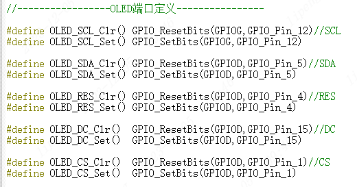
}Modify the OLED port definitions in lcd_init.h to match the style shown in the right image below.
//-----------------OLED Port Definitions----------------
#define OLED_GPIO_PORT      CW_GPIOA
#define OLED_SCL_PIN        GPIO_PIN_5
#define OLED_MOSI_PIN       GPIO_PIN_7
#define OLED_RES_PIN        GPIO_PIN_3
#define OLED_DC_PIN         GPIO_PIN_2
#define OLED_CS_PIN         GPIO_PIN_4

#define OLED_SCL_Clr() GPIO_WritePin(OLED_GPIO_PORT, OLED_SCL_PIN, GPIO_Pin_RESET) // SCL
#define OLED_SCL_Set() GPIO_WritePin(OLED_GPIO_PORT, OLED_SCL_PIN, GPIO_Pin_SET)
#define OLED_SDA_Clr() GPIO_WritePin(OLED_GPIO_PORT, OLED_MOSI_PIN, GPIO_Pin_RESET) // SDA
#define OLED_SDA_Set() GPIO_WritePin(OLED_GPIO_PORT, OLED_MOSI_PIN, GPIO_Pin_SET)
#define OLED_RES_Clr() GPIO_WritePin(OLED_GPIO_PORT, OLED_RES_PIN, GPIO_Pin_RESET) // RES
#define OLED_RES_Set() GPIO_WritePin(OLED_GPIO_PORT, OLED_RES_PIN, GPIO_Pin_SET)
#define OLED_DC_Clr()  GPIO_WritePin(OLED_GPIO_PORT, OLED_DC_PIN, GPIO_Pin_RESET) // DC
#define OLED_DC_Set()  GPIO_WritePin(OLED_GPIO_PORT, OLED_DC_PIN, GPIO_Pin_SET)
#define OLED_CS_Clr()  GPIO_WritePin(OLED_GPIO_PORT, OLED_CS_PIN, GPIO_Pin_RESET) // CS
#define OLED_CS_Set()  GPIO_WritePin(OLED_GPIO_PORT, OLED_CS_PIN, GPIO_Pin_SET)
At this point, the software SPI porting is complete. Please proceed to section 4 for porting verification.
Source Port Definitions
Modified Port Definitions
The software SPI porting is now complete. Please proceed to section 4 for porting verification.3.3.2 Hardware SPI Porting
Compared to software SPI, hardware SPI relies on the hardware SPI controller, where all clock edge sampling, clock generation, and timing control are handled by hardware. This reduces CPU usage and increases operating speed. Software SPI, on the other hand, uses code to control IO output high and low levels, simulating SPI timing, which is slower and less reliable.
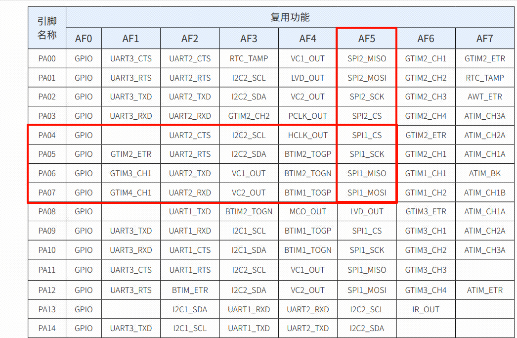
To use hardware SPI to drive the screen, you need to ensure that the selected pins have SPI peripheral functionality. This can be checked in the datasheet.
Note
The datasheet and user manual are available in the Baidu cloud resources; see the introductory manual for the link.
Currently, we are using a hardware SPI interface, and we only need to control the screen without reading data from it. Therefore, we are using a 3-wire SPI, which only requires the clock line SCK, the master output slave input line MOSI, and the software-controlled chip select line NSS. The NSS is controlled by software, so aside from the SCL(SCK)/SDA(MOSI) pins that need to use hardware SPI functionality, other pins can use other GPIOs on the development board. Here, we choose to use the PA5/PA7 SPI multiplexing function. Please connect the other corresponding screen pins as per your requirements. The selected pins are shown in the hardware SPI wiring table.
Wiring Diagram
After selecting the pins, enter the project and start writing the screen pin initialization code.
The pin initialization configuration is shown in the following code.
// OLED Initialization
void OLED_Init(void) {
GPIO_InitTypeDef GPIO_InitStruct; // GPIO initialization structure
__RCC_GPIOA_CLK_ENABLE(); // Enable GPIOA clock
__RCC_SPI1_CLK_ENABLE(); // Enable SPI1 clock
// GPIO multiplexing for SPI1
SPI1_AF_SCK();
SPI1_AF_MOSI();
GPIO_InitStruct.Pins = OLED_SCL_PIN| // GPIO pins
OLED_MOSI_PIN|
OLED_RES_PIN|
OLED_DC_PIN|
OLED_CS_PIN;
GPIO_InitStruct.Mode = GPIO_MODE_OUTPUT_PP; // Push-pull output
GPIO_InitStruct.Speed = GPIO_SPEED_HIGH; // High output speed
GPIO_Init(OLED_GPIO_PORT, &GPIO_InitStruct); // Initialize
SPI_InitTypeDef SPI_InitStructure; // SPI initialization structure
SPI_InitStructure.SPI_Direction = SPI_Direction_2Lines_FullDuplex; // Full duplex
SPI_InitStructure.SPI_Mode = SPI_Mode_Master; // Master mode
SPI_InitStructure.SPI_DataSize = SPI_DataSize_8b; // Frame data length is 8 bits
SPI_InitStructure.SPI_CPOL = SPI_CPOL_High; // Clock idle level is high
SPI_InitStructure.SPI_CPHA = SPI_CPHA_2Edge; // Sample on the second edge
SPI_InitStructure.SPI_NSS = SPI_NSS_Soft; // Chip select signal controlled by SSI register
SPI_InitStructure.SPI_BaudRatePrescaler = SPI_BaudRatePrescaler_8; // Baud rate is PCLK divided by 8
SPI_InitStructure.SPI_FirstBit = SPI_FirstBit_MSB; // Most significant bit MSB transmitted first
SPI_InitStructure.SPI_Speed = SPI_Speed_Low; // Low-speed SPI
SPI_Init(BSP_SPI1, &SPI_InitStructure); // Initialize
SPI_Cmd(BSP_SPI1, ENABLE); // Enable SPI1
OLED_RES_Clr();
delay_ms(200);
OLED_RES_Set();
OLED_WR_Byte(0xAE, OLED_CMD); // Turn off OLED panel
OLED_WR_Byte(0x00, OLED_CMD); // Set low column address
OLED_WR_Byte(0x10, OLED_CMD); // Set high column address
OLED_WR_Byte(0x40, OLED_CMD); // Set start line address (0x00~0x3F)
OLED_WR_Byte(0x81, OLED_CMD); // Set contrast control register
OLED_WR_Byte(0xCF, OLED_CMD); // Set SEG Output Current Brightness
OLED_WR_Byte(0xA1, OLED_CMD); // Set SEG/Column Mapping (0xa0 inverted, 0xa1 normal)
OLED_WR_Byte(0xC8, OLED_CMD); // Set COM/Row Scan Direction (0xc0 inverted, 0xc8 normal)
OLED_WR_Byte(0xA6, OLED_CMD); // Set normal display
OLED_WR_Byte(0xA8, OLED_CMD); // Set multiplex ratio (1 to 64)
OLED_WR_Byte(0x3f, OLED_CMD); // 1/64 duty
OLED_WR_Byte(0xD3, OLED_CMD); // Set display offset
OLED_WR_Byte(0x00, OLED_CMD); // No offset
OLED_WR_Byte(0xd5, OLED_CMD); // Set display clock divide ratio/oscillator frequency
OLED_WR_Byte(0x80, OLED_CMD); // Set divide ratio, Set Clock as 100 Frames/Sec
OLED_WR_Byte(0xD9, OLED_CMD); // Set pre-charge period
OLED_WR_Byte(0xF1, OLED_CMD); // Set Pre-Charge as 15 Clocks & Discharge as 1 Clock
OLED_WR_Byte(0xDA, OLED_CMD); // Set COM pins hardware configuration
OLED_WR_Byte(0x12, OLED_CMD);
OLED_WR_Byte(0xDB, OLED_CMD); // Set VCOMH
OLED_WR_Byte(0x40, OLED_CMD); // Set VCOM Deselect Level
OLED_WR_Byte(0x20, OLED_CMD); // Set Page Addressing Mode (0x00/0x01/0x02)
OLED_WR_Byte(0x02, OLED_CMD);
OLED_WR_Byte(0x8D, OLED_CMD); // Set Charge Pump enable/disable
OLED_WR_Byte(0x14, OLED_CMD); // Set (0x10) disable
OLED_WR_Byte(0xA4, OLED_CMD); // Disable Entire Display On (0xa4/0xa5)
OLED_WR_Byte(0xA6, OLED_CMD); // Disable Inverse Display On (0xa6/a7)
OLED_Clear();
OLED_WR_Byte(0xAF, OLED_CMD);
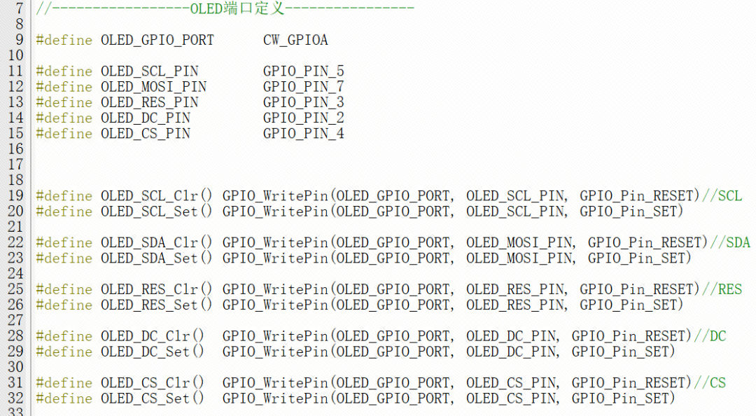
}Modify the LCD port definitions in oled.h to match the style shown in the right images below.
//-----------------OLED Port Definitions----------------
#define BSP_SPI1 CW_SPI1
// GPIO AF
#define SPI1_AF_SCK() PA05_AFx_SPI1SCK()
#define SPI1_AF_MOSI() PA07_AFx_SPI1MOSI()
#define OLED_GPIO_PORT CW_GPIOA
#define OLED_SCL_PIN GPIO_PIN_5
#define OLED_MOSI_PIN GPIO_PIN_7
#define OLED_RES_PIN GPIO_PIN_3
#define OLED_DC_PIN GPIO_PIN_2
#define OLED_CS_PIN GPIO_PIN_4
#define OLED_RES_Clr() GPIO_WritePin(OLED_GPIO_PORT, OLED_RES_PIN, GPIO_Pin_RESET) // RES
#define OLED_RES_Set() GPIO_WritePin(OLED_GPIO_PORT, OLED_RES_PIN, GPIO_Pin_SET)
#define OLED_DC_Clr() GPIO_WritePin(OLED_GPIO_PORT, OLED_DC_PIN, GPIO_Pin_RESET) // DC
#define OLED_DC_Set() GPIO_WritePin(OLED_GPIO_PORT, OLED_DC_PIN, GPIO_Pin_SET)
#define OLED_CS_Clr() GPIO_WritePin(OLED_GPIO_PORT, OLED_CS_PIN, GPIO_Pin_RESET) // CS
#define OLED_CS_Set() GPIO_WritePin(OLED_GPIO_PORT, OLED_CS_PIN, GPIO_Pin_SET)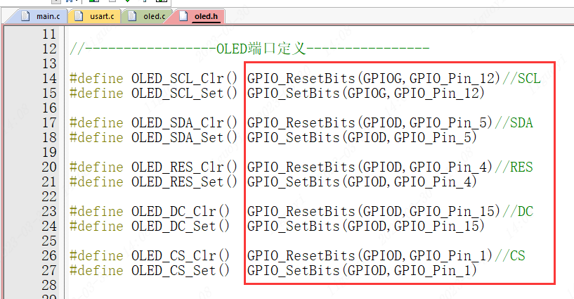 Source Port Definitions
Modified Port Definitions
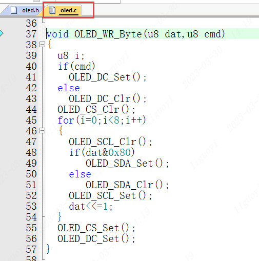
With the initialization part complete, we also need to modify the data sending part. The source code uses software SPI, and the timing is completed by the manufacturer. We need to modify it for hardware SPI.
In the oled.c file, modify the source code function void OLED_WR_Byte(u8 dat,u8 cmd) to match the style shown in the right images below.
Source Code Format
Modified Code
void OLED_WR_Byte(u8 dat,u8 cmd) {
    if(cmd)      OLED_DC_Set();
    else      OLED_DC_Clr();
    OLED_CS_Clr();
    while (SPI_GetFlagStatus(BSP_SPI1, SPI_FLAG_TXE) == RESET);
    SPI_SendData(BSP_SPI1, dat); // Send data
    while (SPI_GetFlagStatus(BSP_SPI1, SPI_FLAG_RXNE) == RESET);
    uint16_t temp = SPI_ReceiveData(BSP_SPI1); // Return data
    OLED_CS_Set();
    OLED_DC_Set();
}
The hardware SPI porting is now complete. Please proceed to section 4 for porting verification.
4. Porting Verification>>>
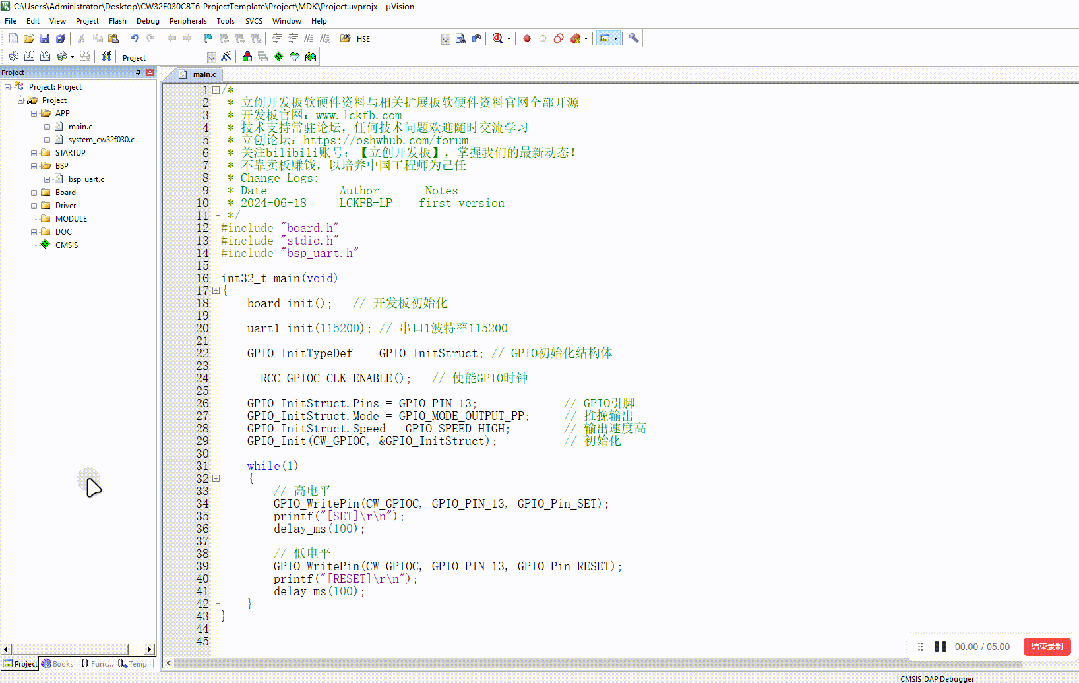
Enter the following code in main.c:
/* * Change Logs: * Date Author Notes * 2024-06-18 LCKFB-LP first version */
#include "board.h"
#include "stdio.h"
#include "bsp_uart.h"
#include "oled.h"
int32_t main(void) {
board_init(); // Development board initialization
uart1_init(115200); // UART1 baud rate 115200
OLED_Init(); // Initialize OLED
OLED_Clear(); // Clear OLED
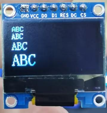
while(1) {
OLED_ShowString(0,0,(uint8_t *)"ABC",8,1); // 6*8 "ABC"
OLED_ShowString(0,8,(uint8_t *)"ABC",12,1); // 6*12 "ABC"
OLED_ShowString(0,20,(uint8_t *)"ABC",16,1); // 8*16 "ABC"
OLED_ShowString(0,36,(uint8_t *)"ABC",24,1); // 12*24 "ABC"
OLED_Refresh();
delay_ms(500);
}
}Power-on effect:
Successful Porting Case (Software and Hardware SPI):
Link:https://pan.baidu.com/s/1qLFWvxXXPbBx4afX4p4KBw?pwd=LCKF
Extraction Code: LCKF
ENDPrevious ReviewsREVIEW
[Product Application] CW32 Electric Tool Product Open Source
[Product Solution] Low-Cost Electric Tool Solution Based on CW32L010
[Product Application] Smart Power Bank Based on CW32 (Open Source Solution)
[Product Application] CW-W88 Water Pump Universal Control Board Design Scheme (Open Source)
[Product Application] Angle Grinder Controller Product Solution Based on CW32
[Product Solution] Low-Voltage Brushless Fan Sensorless Controller Based on CW32F030C8
[Product Solution] Brushless DC Hollow Cup Motor Sensor Control Drive Solution Based on CW32
[Product Solution] Brushless DC Hollow Cup Motor Sensorless Square Wave Control Drive Solution Based on CW32
[Product Solution] Digital Voltage and Current Meter Product Solution Based on CW32F003E4P7
[Product Solution] Low-Cost Industrial Instrument Based on CW32L010
CW32 Ecological Community (WX) Group
 Scan to Join QQ Group4 Group | 478586307
Get materials and “Developer Support Program” first-hand information