1Module Source>>>
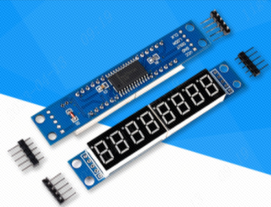
Product Physical Display:
Data Download Link:https://pan.baidu.com/s/15TcV9HevtfVBWcm7pgRNTw
Data Extraction Code:e1q5
2Specifications>>>
Operating Voltage:4-5.5V
Operating Current:8-330MA
Scanning Rate:500-1300Hz
Communication Protocol:Single Bus
Pin Count:5 Pins (2.54mm pitch header)
Refer to the manufacturer’s documentation for the above information
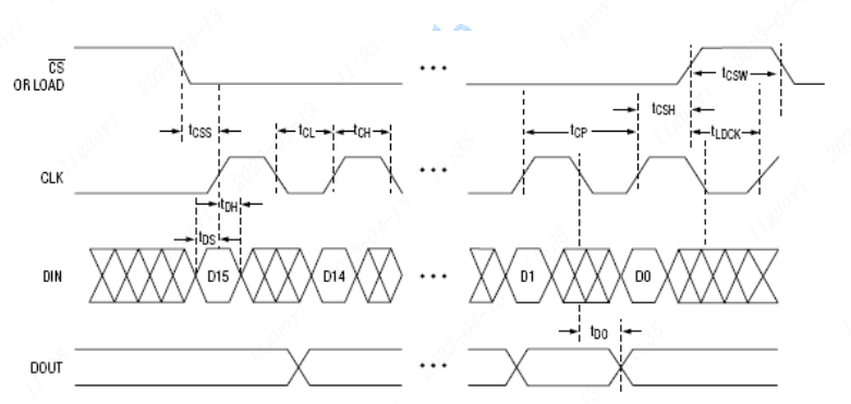
3.1. Timing Explanation
-
Whether data input or output, the CS line must be low. Data is loaded into the data register or control register on the rising edge of the CS line. The CS line must go high after the 16th clock rising edge and before the next clock rising edge; otherwise, data will be lost.
-
For the MAX7219, the serial data is a 16-bit data packet at the DIN input, and data is shifted into the internal 16-bit shift register on the rising edge of CLK. That is, DIN cannot change data on the rising edge of CLK.
3.1.2. Data Bit Explanation
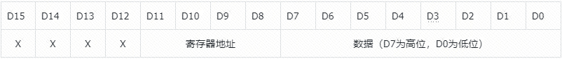
The 16-bit data packet transmitted by DIN is described in Table 000. D8-D11 are the register address bits. D0-D7 are the data bits. D12-D15 are invalid bits.
Based on the above timing explanation and transmission format, the following data transmission code is implemented.
// Write a byte to MAX7219// dat is the data to writevoid Write_Max7219_byte(uint8_t dat){ uint8_t i; MAX7219_CS(0);// Confirm CS is low for(i=8;i>=1;i--)// Transfer 8 bits { MAX7219_CLK(0);// Pull CLK low // Current data bit is 1 if( dat&0x80 ) { MAX7219_DIN(1); } else { MAX7219_DIN(0); } dat=dat<<1;// Prepare the next data bit // CLK goes high to load data into the register MAX7219_CLK(1); }}// Write data to MAX7219// address is the address, dat is the datavoid Write_Max7219(uint8_t address,uint8_t dat){ // Pull CS low MAX7219_CS(0); // Transfer high 8 bits of data (register address) Write_Max7219_byte(address); // Transfer low 8 bits of data (data) Write_Max7219_byte(dat); // Pull CS high MAX7219_CS(1);}3.1.3. Key Register Explanation
Related register addresses are shown in the table below. Here we will first explain the 0X09 decode mode register.
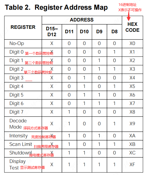
The data bits we send are 16 bits, but only D15-D8 data bits (0x09) are used for the decode mode register, while D7 to D0 are not set. According to the datasheet, the settings for D7-D0 of the decode mode register are in Table 4 of the datasheet.
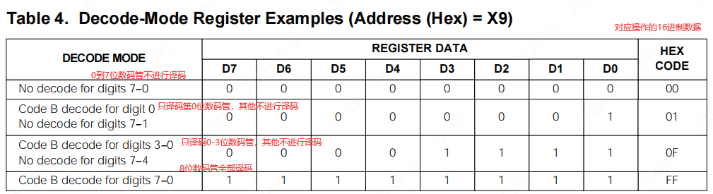
As shown in the figure, if we want to set the decode mode for all 7-segment displays, we need to send:
// High 8 bits = 0x09 (register address), Low 8 bits = 0xff (data)Write_Max7219(0x09,0xff);In the case where all 7-segment displays are decoded, how do we operate if we want the 0th display to show the number 3 and the 1st display to not show anything?
First, find the register addresses for the 0th and 1st displays in the datasheet. According to the right figure, the address for the 0th display is 0X01; the address for the 1st display is 0X02. After knowing the addresses, refer to the data bit setting table in the datasheet. Since all displays are decoded, we only need to send:
// High 8 bits = 0x01 (register address), Low 8 bits = 0x03 (data)Write_Max7219(0x01,0x03);// 0th display shows number 3// High 8 bits = 0x02 (register address), Low 8 bits = 0x0F (data)Write_Max7219(0x02,0x0F);// 1st display does not show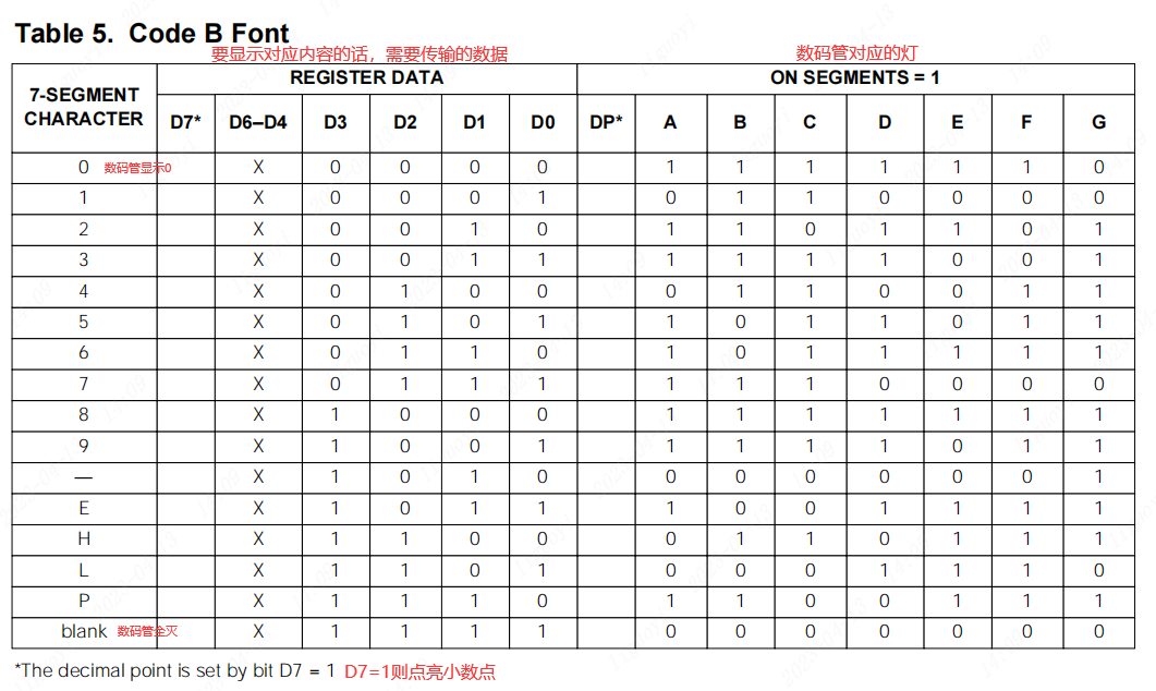
3.2Pin Selection
This module has 10 pins, of which 5 are connected to the next cascaded 7-segment display. If the next cascaded display is not connected, only 5 pins need to be connected. The specific pin connections are shown inPin Connections。
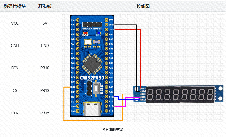
Module Wiring Diagram
3.3Porting to ProjectWe create two files named bsp_max7219.c and bsp_max7219.h and then add the C file to the project and include the path of the header file in the project.https://wiki.lckfb.com/zh-hans/dwx-cw32f030c8t6/module/screen/8-bit-led-tube.html(Click to view the original text with animations)
In the file bsp_max7219.c, write the following code.
/* * Change Logs: * Date Author Notes * 2024-06-18 LCKFB-LP first version */#include "bsp_max7219.h"#include "stdio.h"#include "board.h"/****************************************************************** * Function Name: MAX7219_GPIO_Init * Function Description: Initialize MAX7219 pins * Function Parameters: None * Function Return: None * Author: LC * Notes: None******************************************************************/void MAX7219_GPIO_Init(void){ GPIO_InitTypeDef GPIO_InitStruct; // GPIO initialization structure RCC_MAX7219_ENABLE(); // Enable GPIO clock GPIO_InitStruct.Pins = GPIO_MAX7219_CLK| // GPIO pins GPIO_MAX7219_DIN| GPIO_MAX7219_CS; GPIO_InitStruct.Mode = GPIO_MODE_OUTPUT_PP; // Push-pull output GPIO_InitStruct.Speed = GPIO_SPEED_HIGH; // High output speed GPIO_Init(PORT_MAX7219, &GPIO_InitStruct); // Initialize}/****************************************************************** * Function Name: Write_Max7219_byte * Function Description: Write a byte to MAX7219 * Function Parameters: dat is the data to write * Function Return: None * Author: LC * Notes: None******************************************************************/void Write_Max7219_byte(uint8_t dat){ uint8_t i; MAX7219_CS(0); for(i=8;i>=1;i--) { MAX7219_CLK(0); if( dat&0x80 ) { MAX7219_DIN(1); } else { MAX7219_DIN(0); } dat=dat<<1; MAX7219_CLK(1); }}/****************************************************************** * Function Name: Write_Max7219 * Function Description: Write data to MAX7219 * Function Parameters: address is the address, dat is the data * Function Return: None * Author: LC * Notes: None******************************************************************/void Write_Max7219(uint8_t address,uint8_t dat){ MAX7219_CS(0); Write_Max7219_byte(address); // Write address, i.e., display number 1-8 Write_Max7219_byte(dat); // Write data, i.e., display content MAX7219_CS(1);}/****************************************************************** * Function Name: Write_Max7219_2 * Function Description: Write data to the second MAX7219 * Function Parameters: address is the address, dat is the data * Function Return: None * Author: LC * Notes: Only use if the second MAX7219 is connected******************************************************************/void Write_Max7219_2(uint8_t address,uint8_t dat){ MAX7219_CS(0); Write_Max7219_byte(address); // Write address, i.e., display number 1-8 Write_Max7219_byte(dat); // Write data, i.e., display content MAX7219_CLK(1); Write_Max7219_byte(0X00); // Perform no operation on the first chip Write_Max7219_byte(0X00); MAX7219_CS(1);}/****************************************************************** * Function Name: Write_Max7219_AllOff * Function Description: Turn off all 7-segment displays of the first MAX7219 * Function Parameters: address is the address, dat is the data * Function Return: None * Author: LC * Notes: None******************************************************************/void Write_Max7219_AllOff(void){ int i = 0; for( i = 1; i < 9; i++ ) { MAX7219_CS(0); Write_Max7219_byte(i); // Write address, i.e., display number 1-8 Write_Max7219_byte(15); // Turn off all MAX7219_CS(1); }}/****************************************************************** * Function Name: MAX7219_Init * Function Description: Initialize MAX7219 * Function Parameters: None * Function Return: None * Author: LC * Notes: None******************************************************************/void MAX7219_Init(void){ MAX7219_GPIO_Init(); // Initialize pins Write_Max7219(0x09, 0xff); // Decode mode: BCD code Write_Max7219(0x0a, 0x03); // Brightness Write_Max7219(0x0b, 0x07); // Scan limit; 4 displays show Write_Max7219(0x0c, 0x01); // Power-down mode: 0, normal mode: 1 Write_Max7219(0x0f, 0x01); // Display test: 1; end test, normal display: 0}In the file bsp_max7219.h, write the following code.
/* * Change Logs: * Date Author Notes * 2024-06-18 LCKFB-LP first version */#ifndef _BSP_MAX7219_H_#define _BSP_MAX7219_H_#include "board.h"#define RCC_MAX7219_ENABLE() __RCC_GPIOB_CLK_ENABLE()#define PORT_MAX7219 CW_GPIOB#define GPIO_MAX7219_CLK GPIO_PIN_15#define GPIO_MAX7219_DIN GPIO_PIN_10#define GPIO_MAX7219_CS GPIO_PIN_13#define MAX7219_CLK(X) GPIO_WritePin(PORT_MAX7219, GPIO_MAX7219_CLK, X?GPIO_Pin_SET:GPIO_Pin_RESET)#define MAX7219_DIN(X) GPIO_WritePin(PORT_MAX7219, GPIO_MAX7219_DIN, X?GPIO_Pin_SET:GPIO_Pin_RESET)#define MAX7219_CS(X) GPIO_WritePin(PORT_MAX7219, GPIO_MAX7219_CS, X?GPIO_Pin_SET:GPIO_Pin_RESET)void Write_Max7219(uint8_t address,uint8_t dat);void Write_Max7219_2(uint8_t address,uint8_t dat);void Write_Max7219_AllOff(void);void MAX7219_Init(void);#endif4Porting Verification>>>In the main function of your project, write the following.
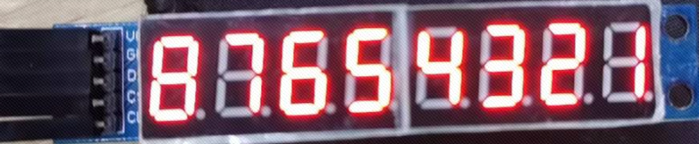
/* * Change Logs: * Date Author Notes * 2024-06-18 LCKFB-LP first version */#include "board.h"#include "stdio.h"#include "bsp_uart.h"#include "bsp_max7219.h"int32_t main(void){ board_init(); // Initialize development board uart1_init(115200); // UART1 baud rate 115200 int i =0; MAX7219_Init(); delay_ms(1000); Write_Max7219(0x0f, 0x00); // Display test: 1; end test, normal display: 0 Write_Max7219_AllOff();// Turn off all displays printf("MAX7219 demo start\r\n"); while(1) { // First display 1, second display 2, third display 3... for( i = 1; i < 9; i++ )// Display from 1 to 8 { Write_Max7219(i, i); delay_ms(1000); } }}Power-on effect:
Successful Porting Case(Software and Hardware SPI):
Link:https://pan.baidu.com/s/1U_l3vfG-S79em6yLpkIWxQ?pwd=LCKF
Extraction Code: LCKF
ENDPrevious ReviewsREVIEW
[Product Application] CW32 Electric Tool Product Open Source
[Product Solution] Low-Cost Electric Tool Solution Based on CW32L010
[Product Application] Smart Power Bank Based on CW32 (Open Source Solution)
[Product Application] CW-W88 Pump Universal Control Board Design Solution (Open Source)
[Product Application] CW32-Based Angle Grinder Controller Product Solution
[Product Solution] Low-Voltage Brushless Fan Sensorless Controller Based on CW32F030C8
[Product Solution] Brushless DC Hollow Cup Motor Sensor Control Drive Solution Based on CW32
[Product Solution] Brushless DC Hollow Cup Motor Sensorless Square Wave Control Drive Solution Based on CW32
[Product Solution] Digital Voltage and Current Meter Product Solution Based on CW32F003E4P7
[Product Solution] Low-Cost Industrial Instrument Based on CW32L010
CW32 Ecological Community (WX) Group
 Scan to Join QQ Group4th Group| 478586307
Get materials and“Developer Support Program”First-hand information