EMMC (Embedded Multi Media Card) is a standard specification established by the MMC Association, primarily targeting embedded storage for products such as mobile phones and tablets. EMMC integrates a controller within the package, providing a standard interface and managing flash memory.The principle circuit’s 8-bit data signals are shown in Figure 8-38, while the address and control signals are shown in Figure 8-39, and the power signals are shown in Figure 8-40. The RK3588 EMMC controller has the following features:
1. Compatible with specifications 5.1, 5.0, 4.51, and 4.41;
2. Supports three data bus widths: 1bit, 4bit, and 8bit;
3. Supports HS400 mode, backward compatible with HS200, DDR50, etc.;
4. Supports CMD Queue.
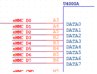
Figure 8-38 EMMC Partial Data Signal Pins
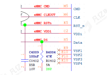
Figure 8-39 EMMC Partial Clock and Control Signals
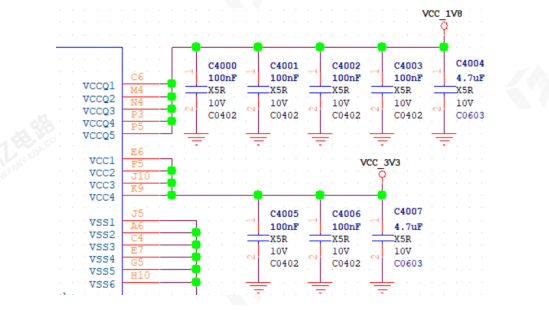
Figure 8-40 EMMC Partial Power Pins
The RK3588 eMMC interface and FSPI Flash (a multiplexed FSPI_M0 interface) are reused. When designing the eMMC interface, please refer to the circuit diagram shown in Figure 8-41 for the eMMC signal connections, which include various power decoupling capacitors. When using eMMC, place the boot code in the eMMC.
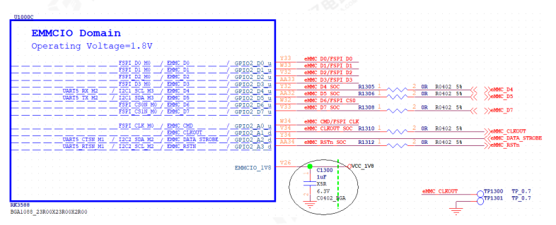
Figure 8-41 Recommended EMMC Circuit Connection Diagram
The recommended pull-up and matching design for the EMMC interface is shown in Table 8-4.
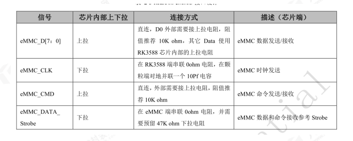
Table 8-4 EMMC Circuit Pull-up and Matching Design
1. The EMMC controller’s pull-down resistors for the clock signal should be placed close to the pins; the clock signal requires grounding treatment, with ground vias every 200mil as shown in Figure 8-42.
2. The data signals, clock signals, and control signals of the EMMC need to maintain a 50-ohm impedance.
3. The filter capacitors for each power pin of the EMMC should be placed close to the corresponding pins, preferably one capacitor per pin, as shown in Figure 8-43.
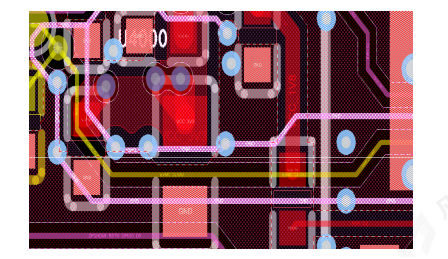
Figure 8-42 CLK Circuit Grounding Schematic
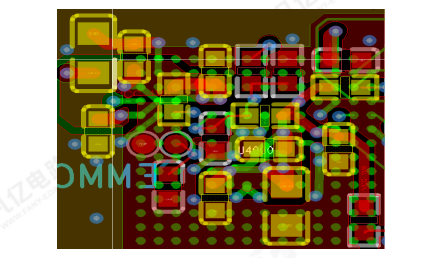
Figure 8-43 Power Filter Capacitor Placement Schematic
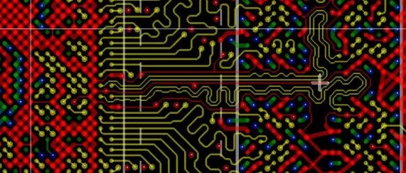
5. The clock, data, and CMD signals need to be serpentine routed to ensure equal length, with a deviation of less than 120mil. The total length of the traces should not exceed 3500mil.
6. The EMMC chip is packaged in a 0.5 pitch BGA package, with many unused pins. The routing can utilize the unused EMMC pins to reduce the requirements for PCB spacing.
7. Minimize layer changes for all EMMC signals, with the number of vias not exceeding two. Before and after layer changes for EMMC signals, it is recommended that the reference layers be ground planes. Within a 30mil range (center-to-center distance between vias) of signal vias, it is advisable to add ground return vias to improve the signal return path. The ground vias should connect the reference ground planes before and after the signal layer change.
PCB Design Recommendations for DDR Modules

EMC Design Check Recommendations for PCB Layout

Scan to add customer service WeChat, note “Join Group” to pull you into the official technical WeChat group of Fanyi Education, to discuss technical issues and insights with many electronic technology experts~