Source: Semiconductor Industry Observation
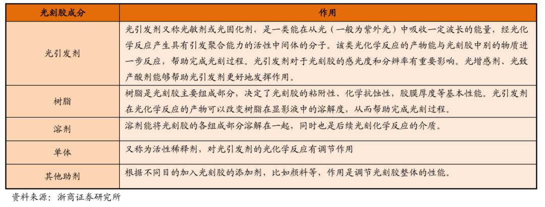
Photoresist, also known as photoresist agent, is a light-sensitive liquid mixture. Its components include: photoinitiators (including photosensitizers and photoacid generators), photoresist resin, monomers, solvents, and other additives. Photoresist can transfer the required fine patterns from a photomask (mask) to the substrate to be processed through photochemical reactions and photolithography processes such as exposure and development. Depending on the application, the substrate to be processed can be integrated circuit materials, display panel materials, or printed circuit boards.
According to statistics from third-party agency Zhiyan Consulting, the global photoresist market size is expected to reach nearly $9 billion in 2019, with a CAGR of about 5.4% from 2010 to present. It is expected that this market will continue to grow at an average rate of 5% per year over the next three years, and by 2022, the global photoresist market size will exceed $10 billion. Photoresists can be classified by application fields into PCB photoresists, display panel photoresists, semiconductor photoresists, and others. The market structure of different types of photoresists is relatively balanced, as shown in the figure below.
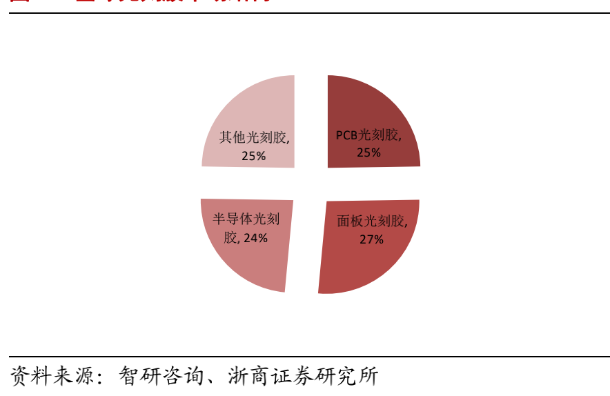
(Global Photoresist Market Structure)
Zhiyan Consulting’s data also shows that benefiting from the trend of the semiconductor, display panel, and PCB industries moving eastward, the annual growth rate of the domestic supply scale of photoresists in China has reached 11% from 2011 to the present, higher than the global average growth rate of 5%. In 2019, the sales scale of domestic enterprises in the Chinese photoresist market was about 7 billion yuan, accounting for about 10% of the global market, indicating great development potential. Currently, domestic photoresists in China are mainly PCB photoresists, while the supply of flat panel display and semiconductor photoresists is extremely low. The production structure of domestic photoresist companies in China can be illustrated as shown below.
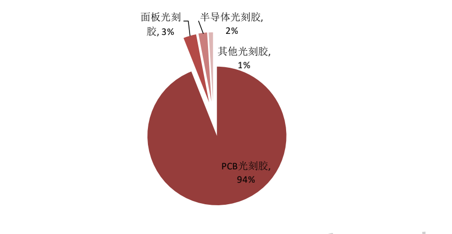
(Production Structure of Domestic Photoresist Companies in China)
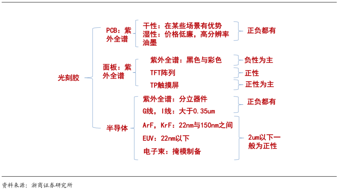
Classification of Photoresists
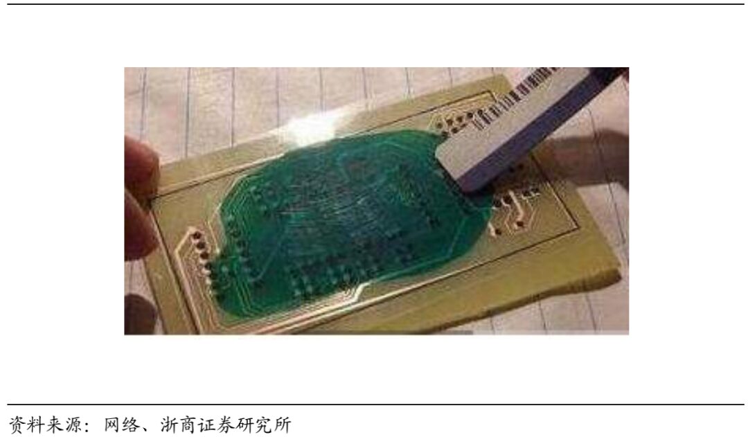
In the flat panel display industry, the main photoresists used are color and black photoresists, LCD touchscreen photoresists, and positive photoresists for TFT-LCD. In the photolithography and etching production processes, photoresist is coated on the surface of the crystalline film, and through exposure, development, and etching processes, the pattern from the photomask is transferred to the film, forming geometric shapes corresponding to the mask.
(Photoresist Coating Process)
In the PCB industry, the main photoresists used are dry film photoresists, wet film photoresists, and photosensitive solder mask inks. Dry film is a special thin film applied to treated copper-clad boards for exposure and development; wet film and photo-imaging solder mask inks are coated on the copper-clad boards, and after drying, they undergo exposure and development. Both dry and wet films have their advantages; generally speaking, wet film photoresists have a higher resolution than dry films and are more economical, gradually replacing some of the market share of dry film photoresists.
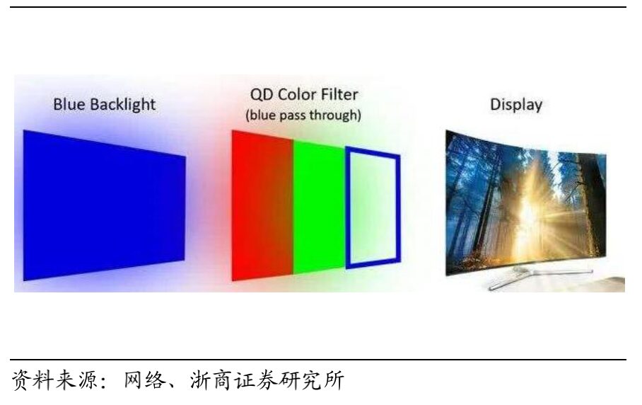
(Color Filter Manufacturing for LCD Screens Relies on Color Photoresists)
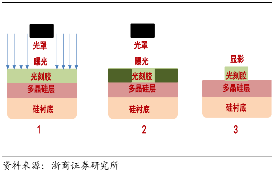
In the semiconductor integrated circuit manufacturing industry, the main photoresists used are g-line photoresists, i-line photoresists, KrF photoresists, and ArF photoresists. In the manufacturing process of large-scale integrated circuits, silicon wafers generally undergo more than ten photolithography steps. In each photolithography and etching process, photoresist must go through pre-baking, coating, post-baking, alignment, exposure, post-baking, development, and etching to transfer the pattern from the photomask to the silicon wafer.
(Photoresist Development Diagram)
Photoresist is an important material in integrated circuit manufacturing: the quality and performance of photoresist are key factors affecting the performance, yield, and reliability of integrated circuits. The cost of photolithography processes accounts for about 35% of the total chip manufacturing process, and the time consumed accounts for approximately 40%-50% of the entire chip process. Photoresist materials account for about 4% of the total cost of IC manufacturing, indicating a vast market. Therefore, photoresist is a core material in semiconductor integrated circuit manufacturing.
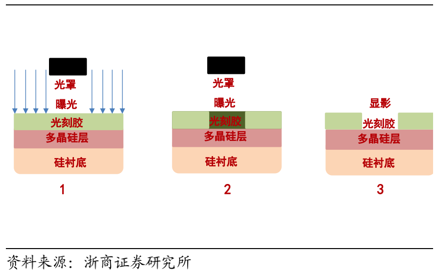
(Positive Photoresist Development Diagram)
Classified by display effect, photoresists can be divided into positive and negative photoresists. The pattern formed by negative photoresists during development is the opposite of that of the photomask; positive photoresists form patterns that are the same as the mask. The production processes of both are basically the same, differing primarily in the main raw materials.
(Negative Photoresist Development Diagram)
According to chemical structure classification, photoresists can be divided into photopolymerization type, photodecomposition type, photocrosslinking type, and chemically amplified type. Photopolymerization photoresists use olefin monomers to generate free radicals under light, further initiating monomer polymerization, ultimately forming polymers;
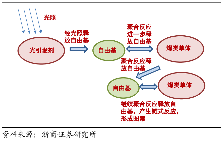
(Photopolymerization Reaction Diagram)
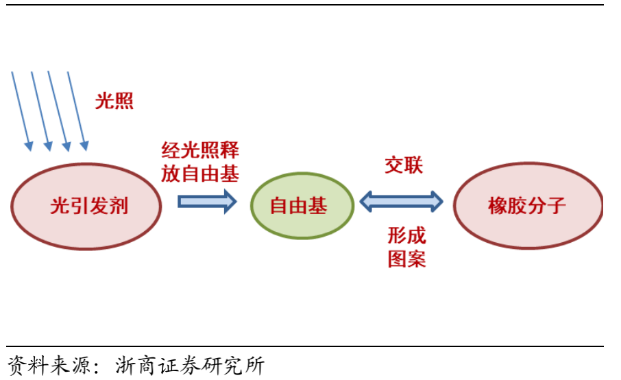
Photodecomposition photoresists use diazonaphthoquinone (DNQ) materials as photosensitizers, which undergo photodecomposition reactions upon exposure, allowing for the creation of positive photoresists; photocrosslinking photoresists use polyvinyl alcohol laurate and other materials as photosensitive materials, forming an insoluble network structure under light, thus providing etching resistance, allowing for the creation of negative photoresists.
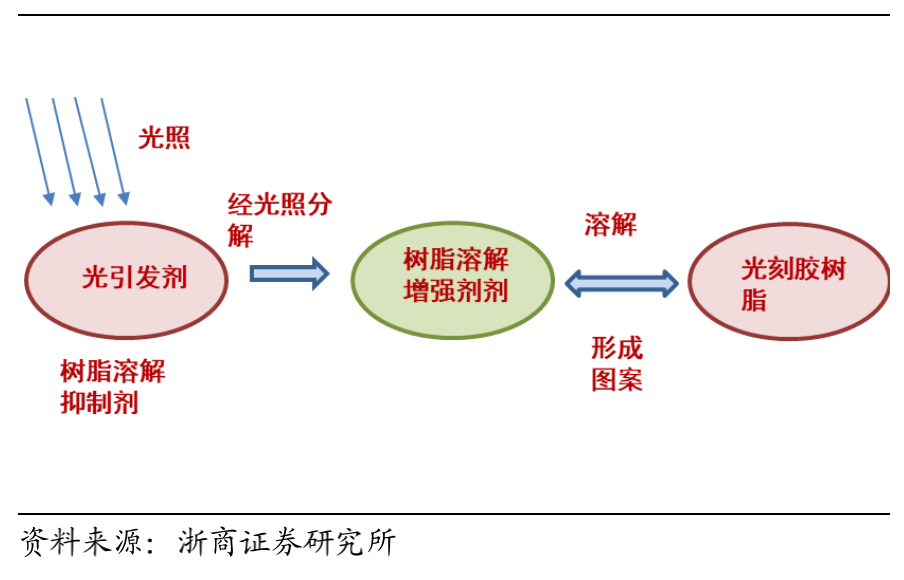
(Photodecomposition Reaction Diagram)
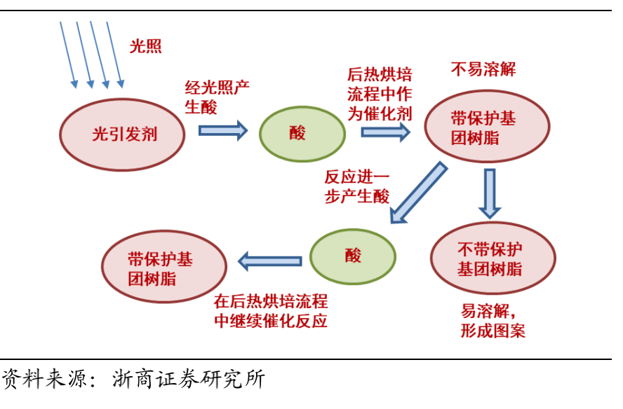
Since the introduction of deep ultraviolet (DUV) light sources in semiconductor integrated circuit photolithography technology, chemically amplified (CAR) technology has gradually become mainstream in the industry. In chemically amplified photoresists, the resin is polyethylene with protected chemical groups that are difficult to dissolve. Chemically amplified photoresists use photoacid generators (PAGs) as photoinitiators.
(Chemical Crosslinking Reaction Diagram)
When photoresist is exposed, the photoacid generator (PAG) in the exposed area will produce an acid. This acid acts as a catalyst during the subsequent thermal baking process, removing the protective groups from the resin, making it easier for the resin to dissolve. The exposure sensitivity of chemically amplified photoresists is ten times that of DNQ photoresists, exhibiting good optical sensitivity to deep ultraviolet light, high contrast, and high resolution among other advantages.
(Chemically Amplified Light Reaction Diagram)
Classified by exposure wavelength, photoresists can be divided into ultraviolet photoresists (300~450nm), deep ultraviolet photoresists (160~280nm), extreme ultraviolet photoresists (EUV, 13.5nm), electron beam photoresists, ion beam photoresists, and X-ray photoresists. The applicable photolithography resolution limits differ for photoresists with different exposure wavelengths. Generally speaking, under the same process conditions, the shorter the wavelength, the better the processing resolution.
(Summary of Photoresist Classification)
Photoresist is the “Fuel” for the Advancement of Semiconductor Process Technology
In the field of integrated circuit manufacturing, if photolithography machines are the “engines” driving the advancement of process technology, photoresists are the “fuel” for these engines. The following diagram illustrates how photoresists play a role in the manufacturing process of an NMOS transistor. NMOS transistors are one of the most commonly used integrated circuit structures in semiconductor process technology.
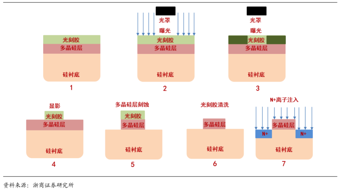
(Manufacturing Process of an NMOS Transistor Integrated Circuit Structure)
In this typical example, the green area in step 1 represents the area where the red polysilicon material is coated with a layer of photoresist. During the photolithography exposure process in step 2, the photoresist outside the black mask is irradiated by the photolithography light source, causing a chemical change, which is reflected in step 3 as it turns dark green. In step 4, after development, only the areas above the red polysilicon material that were previously masked are left with photoresist material.
Thus, the pattern from the photomask is transferred to the polysilicon material, completing the photolithography process. In subsequent steps 5 to 7, based on the photoresist pattern left on the polysilicon material from the photolithography process, the processes of “polysilicon etching,” “photoresist cleaning,” and “N+ ion implantation” together complete the construction of an NMOS transistor.
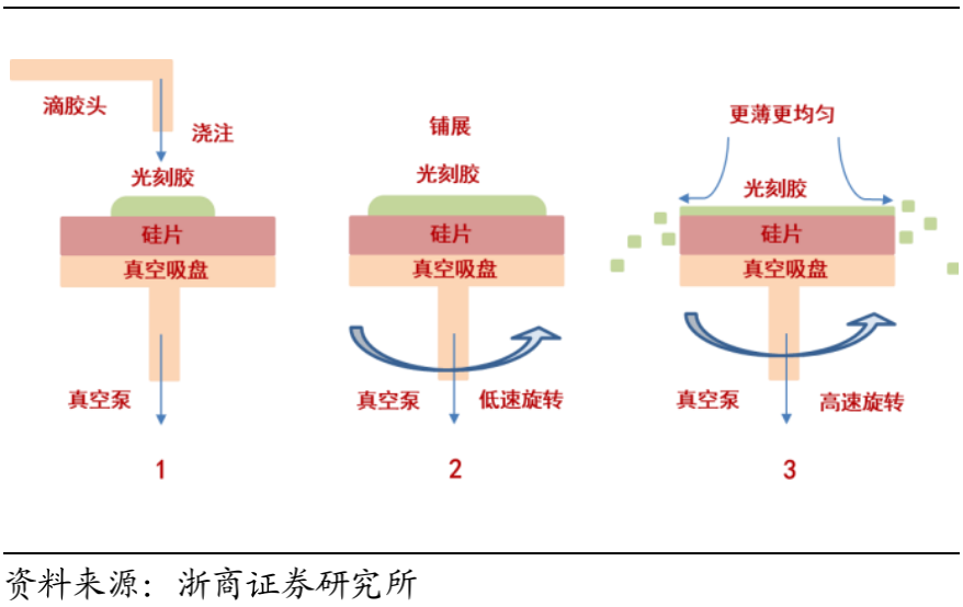
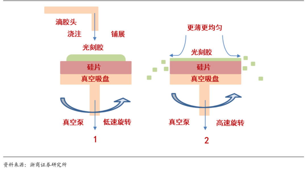
The photoresist coating process in step 1 is also an important semiconductor process. The purpose is to establish a thin, uniform, and defect-free photoresist film on the wafer surface. Generally, the thickness of the photoresist film ranges from 0.5um to 1.5um, with a thickness error required to be within ±0.01um. The main coating method for semiconductor photoresists is the spin coating method, which can be further divided into static spin coating and dynamic spray coating.
(Static Spin Coating Process Diagram)
Static spin coating: First, the photoresist is deposited in the center of the silicon wafer using a dispensing head, then rotated at low speed to spread the photoresist, and finally spun at high speed to remove excess photoresist. During the high-speed rotation, some of the solvents in the photoresist will evaporate. This process can be illustrated as shown in the figure. The amount of photoresist deposited in static spin coating is very critical; too little will lead to insufficient coverage of the silicon wafer, while too much will cause the photoresist to accumulate at the edges of the wafer or even flow to the back of the wafer, affecting process quality.
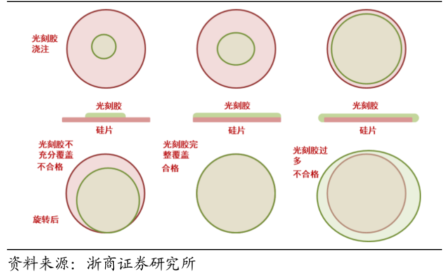
(Qualified vs. Unqualified Static Coating Process Diagram)
Dynamic spray coating: As wafer sizes have increased, static coating can no longer meet the latest silicon wafer processing needs. Compared to static spin coating, dynamic spray coating begins to help the photoresist spread at low speed right when the photoresist is poured onto the wafer. This method can form a more uniform photoresist spread with a smaller amount of photoresist, ultimately achieving a photoresist film that meets thickness and uniformity requirements through high-speed rotation.
(Dynamic Spray Coating Process Diagram)
As the integration level of ICs increases, the process technology level of integrated circuits has transitioned from micrometer, sub-micrometer, and deep sub-micrometer to the nanometer stage. The trend of continuously shrinking integrated circuit line widths poses new challenges to semiconductor process technologies, including photolithography. The critical dimension (CD) of integrated circuit line widths can be determined by the Rayleigh formula as shown:
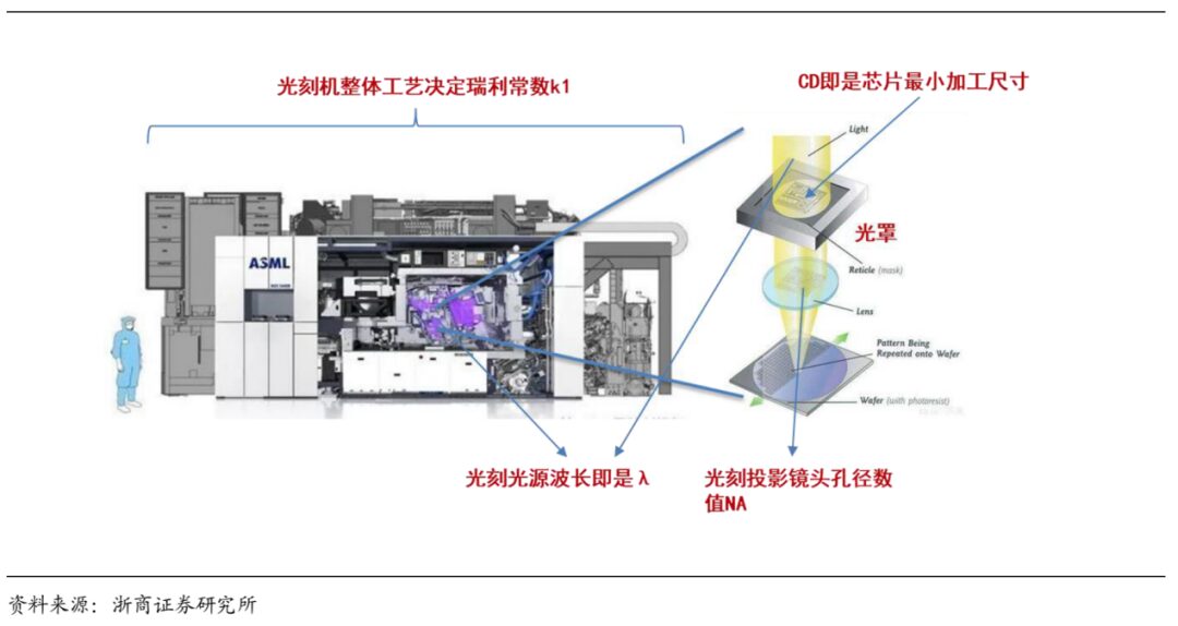
(Meaning of Parameters in Rayleigh Formula)
CD (Critical Dimension) represents the feature size in integrated circuit processes; k1 is the Rayleigh constant, a correlation coefficient of processes and materials in photolithography systems; λ is the exposure wavelength, while NA (Numerical Aperture) represents the numerical aperture of the photolithography machine. Therefore, photolithography machines need to manufacture integrated circuits with smaller feature sizes by reducing the Rayleigh constant and exposure wavelength and increasing the aperture size. Reducing the exposure wavelength is closely related to the light source used in the photolithography machine and the photoresist materials.
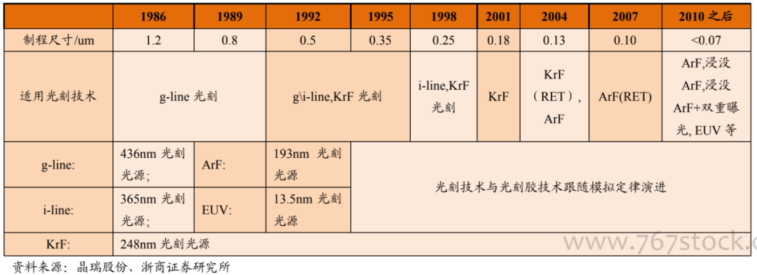
Historically, the wavelengths of light sources used in photolithography machines have shown a trend of shrinking in sync with the critical dimensions of integrated circuits. Different wavelengths of photolithography light sources require completely different photolithography equipment and photoresist materials. In the 1980s, the mainstream process dimensions of semiconductor fabrication were between 1.2um (1200nm) and 0.8um (800nm). At that time, a light source with a wavelength of 436nm was widely used. In the first half of the 1990s, as semiconductor process dimensions evolved towards 0.5um (500nm) and 0.35um (350nm), photolithography began to adopt light sources with a wavelength of 365nm.
436nm and 365nm light sources are the two spectral lines with the highest energy and shortest wavelengths in high-pressure mercury lamps. High-pressure mercury lamp technology is mature, thus it was the first to be used as a photolithography light source. Using light sources with shorter wavelengths and higher energy makes it easier to excite photochemical reactions and improve photolithography resolution. The modern German scientist Joseph von Fraunhofer, known for his research on spectra, named these two wavelengths G line and I line, which is also the origin of the names g-line lithography and i-line lithography technology.
Both g-line and i-line photoresists use linear phenolic components as the main resin and diazonaphthoquinone (DNQ) components as photosensitizers. The unexposed DNQ components act as inhibitors, significantly reducing the dissolution rate of photoresists in the developer. After exposure, the diazonaphthoquinone (DNQ) groups convert to enones, which further transform into indene carboxylic acid upon contact with water, allowing the exposed photoresist to be removed during development with weak alkaline water, while the unexposed portions remain. Although g-line and i-line photoresists use similar components, their resins and photosensitizers have variations at the microscopic level, resulting in different resolutions. G-line photoresists are suitable for the fabrication of integrated circuits with sizes above 0.5um (500nm), while i-line photoresists are used for integrated circuits ranging from 0.35um (350nm) to 0.5um (500nm).
Additionally, both types of photoresists can be used for the manufacturing of larger electronic products such as LCD panels.
In the late 1990s, following Moore’s Law, the process dimensions of semiconductor fabrication began to shrink below 0.35um (350nm), necessitating higher resolution photolithography technologies. Deep ultraviolet light, due to its shorter wavelength and reduced diffraction effects, can be used for higher resolution photolithography light sources. With the development of KrF and ArF rare gas halide excimer laser light sources, photolithography light source technology at wavelengths of 248nm (KrF) and 193nm (ArF) began to mature and be put into practical use.
However, due to the strong absorption effects of DNQ system photoresists in the deep ultraviolet wavelength band, the light emitted by KrF and ArF as photolithography gases cannot penetrate DNQ photoresists, which means that photolithography resolution would be severely impacted. Therefore, deep ultraviolet photoresists adopt a completely different technical system from i-line and g-line photoresists, referred to as the chemically amplified resist (CAR) system.
In the CAR technical system, the photoinitiators in photoresists do not directly change the solubility of the photoresists in the developer upon exposure but instead generate acids. Under the high-temperature conditions of subsequent thermal baking processes, the acids generated during exposure act as catalysts to alter the solubility of photoresists in the developer. Therefore, the photoinitiators in CAR photoresists are also known as photoacid generators.
Since the acids generated by the photoacid generators in CAR photoresists do not get consumed during exposure but merely exist as catalysts, a small amount of acid can continuously exert effective action. CAR photoresists are highly sensitive to light, requiring very little energy from deep ultraviolet radiation to absorb, greatly enhancing photolithography efficiency. The exposure sensitivity of CAR photoresists is about ten times that of DNQ photoresists.
Since the latter half of the 1990s, photolithography light sources have begun to adopt KrF lasers with a wavelength of 248nm; starting from the 2000s, photolithography has further shifted to using ArF excimer lasers with a wavelength of 193nm as the light source. Since then, for approximately 20 years, ArF excimer lasers at a wavelength of 193nm have remained the most reliable and widely used photolithography light sources in the semiconductor process field.
Generally speaking, KrF (248nm) photoresists use polyhydroxystyrene and its derivatives as film-forming resins, and use sulfonic acid iodide and sulfonic acid salts as photoacid generators; while ArF (193nm) photoresists often use derivatives of polymethyl methacrylate, cyclic olefin-maleic anhydride copolymers, and cyclic polymers as film-forming resins. Due to structural reasons, ArF (193nm) photoresists require more sensitive photoacid generators than KrF (248nm) photoresists.
Although after 2007, some excimer lithography light source technologies with shorter wavelengths have emerged, the radiation in these bands is easily absorbed by optical materials such as photolithography lenses, causing these materials to heat up and expand, preventing them from functioning normally. A few optical materials that can work normally with these bands of radiation, such as calcium fluoride (fluorite), have remained prohibitively expensive. Coupled with the emergence of new technologies such as immersion lithography and multiple exposures, the 193nm wavelength ArF lithography system has broken through the previous 65nm resolution bottleneck, thus remaining widely applied in semiconductor process technologies between 45nm and 10nm.
(Evolution of Photolithography Light Source Technology)
Immersion lithography: In contrast to dry lithography, where the space between the photolithography lens and the photoresist is air, in immersion lithography, there is a specific liquid between the photolithography lens and the photoresist. This liquid can be pure water or other compounds. The radiation emitted by the photolithography light source refracts through these liquids, shortening the wavelength. Thus, without changing the light source, shorter wavelength ultraviolet light is projected onto the photoresist, improving the resolution of photolithography processing. The left diagram shows a typical immersion lithography system.
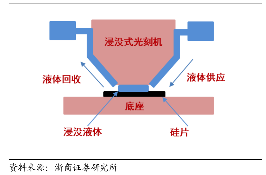
(Typical Immersion Lithography System)
Double exposure lithography: Double exposure lithography means that processing resolution is doubled by performing photolithography twice. One method to achieve this is to shift the same photomask after the first photolithography to perform a second photolithography, thereby enhancing processing resolution. The right diagram illustrates this process. In the right diagram, double exposure lithography involves two coating processes, two photolithography processes, and two etching processes. With advancements in photoresist technology, it has also become possible to achieve double exposure lithography with only one coating, two photolithography processes, and one etching process.
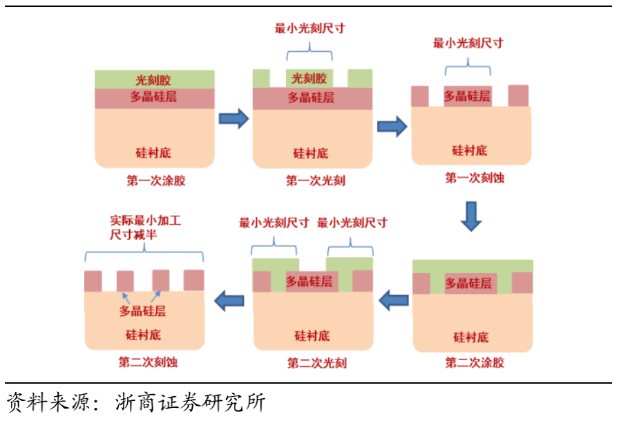
(Double Exposure Doubles Processing Resolution)
Immersion lithography and double exposure lithography technologies push processing resolutions towards the 10nm scale without changing the 193nm wavelength ArF photolithography light source. At the same time, these two technologies impose new requirements on photoresists. In immersion processes, photoresists must not chemically react with the immersion liquid or diffuse out, damaging the photoresist and the photolithography lens; additionally, the refractive index of the photoresist must be greater than that of the lens, liquid, and top coating. Therefore, the refractive index of the main resin in photoresists is generally required to reach above 1.9; furthermore, photoresists must not deform during soaking in the immersion liquid and subsequent baking processes, which could affect processing accuracy; finally, as the target resolution of immersion processes approaches 10nm, the trade-offs for multiple performance indicators of photoresists become increasingly stringent. Immersion ArF photoresists are more challenging to prepare than dry ArF photoresists, which is one of the key factors for breaking through the 45nm resolution in ArF lithography processing.
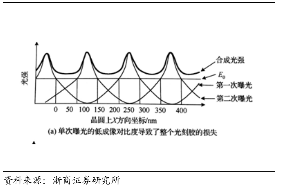
(Unqualified Double Exposure)
In double exposure lithography, if the photoresist can accept multiple exposures without undergoing photochemical reactions in the non-masked areas, one etching, one coating, and one photoresist cleaning process can be saved. The left diagram shows an unqualified double exposure process. Due to the relatively small amount of radiation the photoresist receives in the non-exposed areas, after two exposures, the radiation received in the non-exposed areas may exceed the exposure threshold E0, resulting in incorrect photolithography reactions. In the right diagram, the radiation energy received by the photoresist in the non-exposed areas after two exposures remains below its exposure threshold E0, thus the right diagram illustrates a qualified double exposure. This example shows that, unlike single exposure, double exposure requires a balance between the exposure threshold of the photoresist and the intensity of the light source.
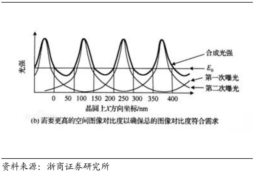
(Qualified Double Exposure)
EUV (Extreme Ultraviolet) lithography technology is the latest advancement in the photolithography field over the past 20 years. Currently, available optical materials cannot adequately support the reflection and transmission of radiation below a wavelength of 13nm, thus EUV lithography technology uses ultraviolet light with a wavelength of 13.5nm as the photolithography light source. EUV lithography technology continues to advance semiconductor process technology in the sub-10nm region. At the 13.5nm wavelength scale of EUV lithography processes, quantum uncertainty effects begin to manifest, presenting unprecedented challenges for the design and use of corresponding light sources, photomasks, and photoresists. Currently, only ASML in the Netherlands has the capability to manufacture EUV lithography machines, and many corresponding technical details remain unknown to the outside world. In the upcoming EUV lithography era, the industry anticipates a comprehensive technological revolution for the KrF and ArF photoresist technologies that have been prevalent for the past 20 years.
High Barriers in Photoresist Material Preparation
Photoresists belong to the field of microelectronic chemicals, which intersects the electronics and chemical industries, representing a typical technology-intensive industry. Engaging in microelectronic chemical business requires key production technologies that match the cutting-edge developments in the electronics industry, such as mixing technology, separation technology, purification technology, and corresponding analytical testing, environmental treatment, and monitoring technologies. Additionally, the diverse application scenarios in the downstream electronics industry require microelectronic chemical production enterprises to have strong supporting capabilities to promptly develop and improve product processes to meet customer-specific needs.
The main process of photoresist production involves mixing photosensitive materials, resins, solvents, and other raw materials in a cleanroom environment of 1000-level yellow light area at constant temperature and humidity, fully stirring under nitrogen gas protection to create a homogeneous liquid, followed by multiple filtration, and intermediate process control and testing to meet technical and quality requirements before product inspection, packaging, labeling, and storage under nitrogen gas protection. The entire process flow can be illustrated as shown:
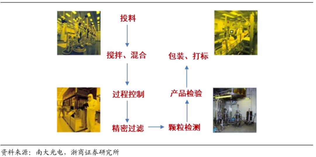
(Brief Process Flow of Photoresist Production)
The technical barriers of photoresists include formulation technology, quality control technology, and raw material technology. Formulation technology is the core of achieving functionality in photoresists, while quality control technology ensures the stability of photoresist performance, and high-quality raw materials form the foundation of photoresist performance.
Formulation technology: Since the downstream users of photoresists are IC chip and FPD panel manufacturers, different customers have different application needs, and the same customer may have varying photoresist application requirements. Generally, a semiconductor chip requires 10-50 photolithography processes during its manufacturing. Due to differences in substrates, resolution requirements, and etching methods, the specific requirements for photoresists vary across different photolithography processes, and even similar photolithography processes may have different requirements from different manufacturers. Addressing these diverse application needs results in a wide variety of photoresists, with these differences primarily achieved by adjusting the formulations of the photoresists. Therefore, adjusting the formulations of photoresists to meet differentiated application needs is the core technology for photoresist manufacturers.
Quality control technology: Given the high demands for stability and consistency in photoresists, including consistency between different batches, users typically hope to maintain a high level of consistency in photosensitivity and film thickness. Thus, photoresist manufacturers must not only have complete testing instruments but also establish a rigorous QA system to ensure product quality stability.
Raw material technology: Photoresists are complex and precisely formulated products designed through different combinations of film-forming agents, photosensitizers, solvents, and additives. The quality of photoresist raw materials plays a critical role in the quality of the photoresists. The purity of semiconductor chemical reagents is subject to international standards set by the Semiconductor Equipment and Materials International (SEMI), as shown in the table below.
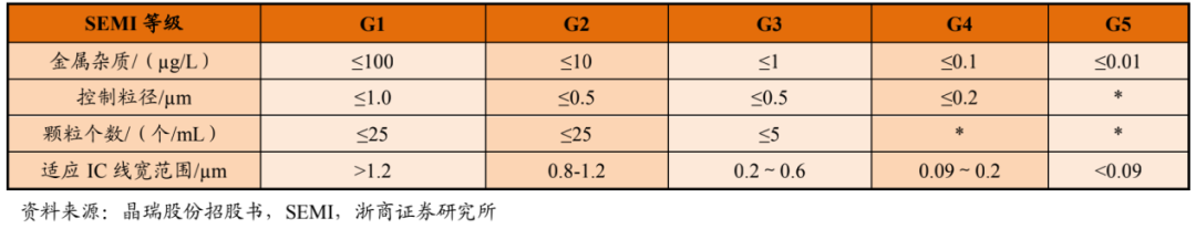
(SEMI Ultra Clean High Purity Reagent Standards)
The purity requirements for reagents and materials used in semiconductor integrated circuits are high, primarily concentrated at SEMI G3 and G4 levels. There remains a significant gap between our R&D levels and international standards; the purity requirements for ultra-clean high-purity reagents for semiconductor discrete devices are lower than those for integrated circuits, primarily concentrated at SEMI G2 levels, and domestic companies can meet most production needs; the purity requirements for ultra-clean high-purity reagents in flat panel display and LED fields are at SEMI G2 and G3 levels, which domestic companies can also meet for most production needs.
Microelectronic chemicals, including photoresists, exhibit high technical requirements, strong functionality, and rapid product updates, significantly impacting the quality and efficiency of downstream electronic products. Consequently, downstream enterprises place great importance on the quality and supply capabilities of microelectronic chemical suppliers, often adopting an accredited procurement model, requiring strict selection processes through sample testing, technical discussions, feedback, technical improvements, small batch trials, large-scale supply, and after-sales service evaluations.
Certification processes are lengthy and demanding; generally, it takes a long time for products to receive certification from downstream customers. The display panel industry typically takes 1-2 years, while the integrated circuit industry, due to its higher requirements, can take 2-3 years; during the certification phase, photoresist suppliers do not earn revenue from that customer, necessitating sufficient financial strength.
Photoresist suppliers have high customer stickiness; typically, to maintain stable supply and performance of photoresists, once downstream customers establish supply relationships with photoresist suppliers, they are unlikely to switch easily. By establishing feedback mechanisms and meeting personalized needs, the stickiness between photoresist suppliers and customers continues to increase. New entrants wishing to join the supplier ranks often need to meet higher requirements than existing suppliers. Thus, the photoresist industry presents high barriers to new entrants.
Generally, microelectronic chemicals such as photoresists not only have high quality requirements but also need to meet diverse needs of downstream customers. Without economies of scale, suppliers cannot afford the costs associated with meeting high-quality diversified demands. Therefore, product variety and scale constitute significant barriers to entry into this industry.
Moreover, microelectronic chemicals generally exhibit certain corrosiveness, imposing high requirements on production equipment, and production environments must undergo dust-free or micro-dust treatment. The preparation of high-end microelectronic chemicals requires fully enclosed and automated production processes to avoid contamination and enhance quality. Consequently, the production of microelectronic chemicals such as photoresists necessitates high standards in safety production, environmental protection equipment, production process systems, process control systems, and R&D investments. Without substantial financial strength, enterprises struggle to gain competitive advantages in equipment, R&D, and technical services, thereby enhancing sustainable development capabilities. Therefore, the microelectronic chemicals industry, exemplified by photoresists, has significant financial barriers.
Market Dominated by the US and Japan
The photoresist industry has extremely high barriers to entry, resulting in an oligopolistic situation globally. The photoresist industry has long been dominated by specialized companies from Japan and the United States. Currently, the top five manufacturers account for 87% of the global photoresist market share, indicating a high industry concentration. Among them, Japanese companies such as JSR, Tokyo Ohka Kogyo, Shin-Etsu Chemical, and Fujifilm account for a combined market share of 72%. Furthermore, the core technologies for high-resolution KrF and ArF semiconductor photoresists are primarily monopolized by Japanese and American companies, with the majority of products originating from companies such as DuPont, JSR Corporation, Shin-Etsu Chemical, Tokyo Ohka Kogyo, Fujifilm, and Korea’s Dongjin. Overall, Japan serves as a hub for major players in the photoresist industry.
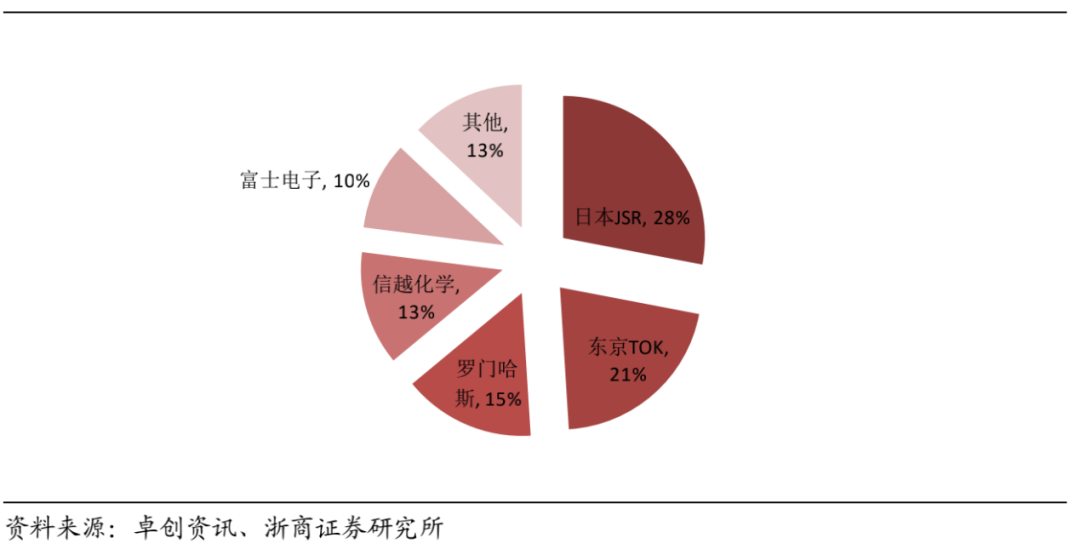
(Market Share of Global Photoresist Production Companies)
Japan-Korea Material Friction: The localization of semiconductor materials is an inevitable trend; in July 2019, against the backdrop of Japan-Korea trade disputes, Japan announced a ban on three semiconductor materials for South Korea, including etching gases, photoresists, and fluorinated polyimides. South Korea is a global hub for memory and display production, and a large number of wafer foundries and display manufacturers, such as Samsung, SK Hynix, and Dongbu HiTek, require Japanese semiconductor materials. These three materials directly cut off the economic lifelines of South Korea’s memory and display sectors.
After the ban, South Korea’s semiconductor industry faced an unprecedented crisis, with global memory leaders such as Samsung and SK Hynix at risk of production stoppage, as Samsung’s material inventory could only sustain production for three months. Executives from Samsung and SK Hynix frequently negotiated with Japan. If relations between Japan and Korea, both important allies of the United States, are so strained, the developing Chinese technology industry must heed this warning.
Currently, mainland China relies heavily on foreign sources for electronic materials, especially in the area of photoresists. Therefore, domestic substitution for semiconductor materials is an inevitable trend.
China-US Trade Friction: Domestic substitution of photoresists is an urgent need for China’s semiconductor industry; since the onset of China-US trade friction, mainland China has actively laid out its integrated circuit industry. In the field of semiconductor materials, photoresists are the “fuel” for advancements in integrated circuit process technologies and are a crucial link in domestic substitution, which is bound to be localized.
Photolithography is the core process in semiconductor fabrication, playing a decisive role in producing more advanced integrated circuits with higher transistor densities. Each generation of new photolithography processes requires a corresponding generation of photoresist technology. Currently, a semiconductor chip typically undergoes 10-50 photolithography processes during its manufacturing. Different photolithography processes impose varying specific requirements on photoresists; if the performance of photoresists does not meet standards, it can significantly impact chip yield.
Currently, China’s level of photoresist localization is severely inadequate, with significant technology gaps in the semiconductor photoresist sector, reflecting a 2-3 generation gap. With the rapid development of downstream semiconductor, LED, and flat panel display industries, there is enormous potential for domestic photoresist product localization in the future. Today, China is leveraging the National Integrated Circuit Industry Investment Fund (Big Fund) to mobilize social resources for investment and support in the semiconductor industry.
At the same time, domestic photoresist companies are seizing the century-long opportunity of expanding wafer manufacturing in China, developing photoresist businesses to strive to catch up to international advanced levels and enter the supply chains of newly established domestic wafer fabs. The localization of photoresists is being comprehensively promoted, and in the field of panel display photoresists, several competitive domestic enterprises have already emerged.
In the semiconductor and panel display photoresist sectors, although domestic photoresists still lag behind international advanced levels, supported by policies and relentless efforts, several domestic photoresist companies have begun to achieve technological breakthroughs.
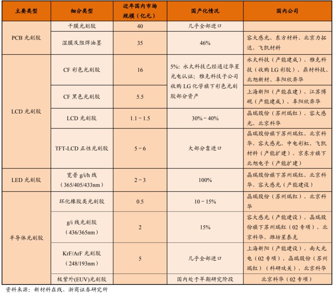
(Major Domestic Photoresist Producers and Localization Status)
Public Account ID:imecas_wx