Source: Semika
Original Author: Semika
This article introduces the process of lithography, the basic principles of lithography machines, as well as the characteristics and applications of various lithography machines.
The Process of Lithography
Lithography is a pattern transfer technology that transfers the graphics on a mask to a silicon wafer coated with photoresist (also known as photoresist). Through a series of production steps, specific parts of the thin film on the surface of the silicon wafer are removed.
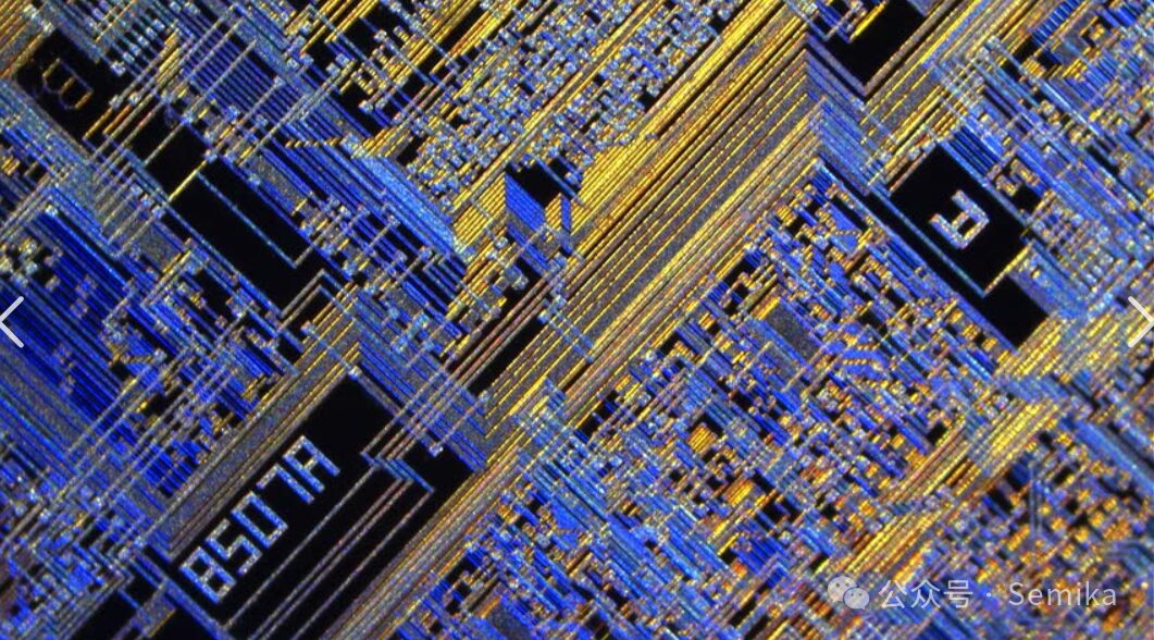
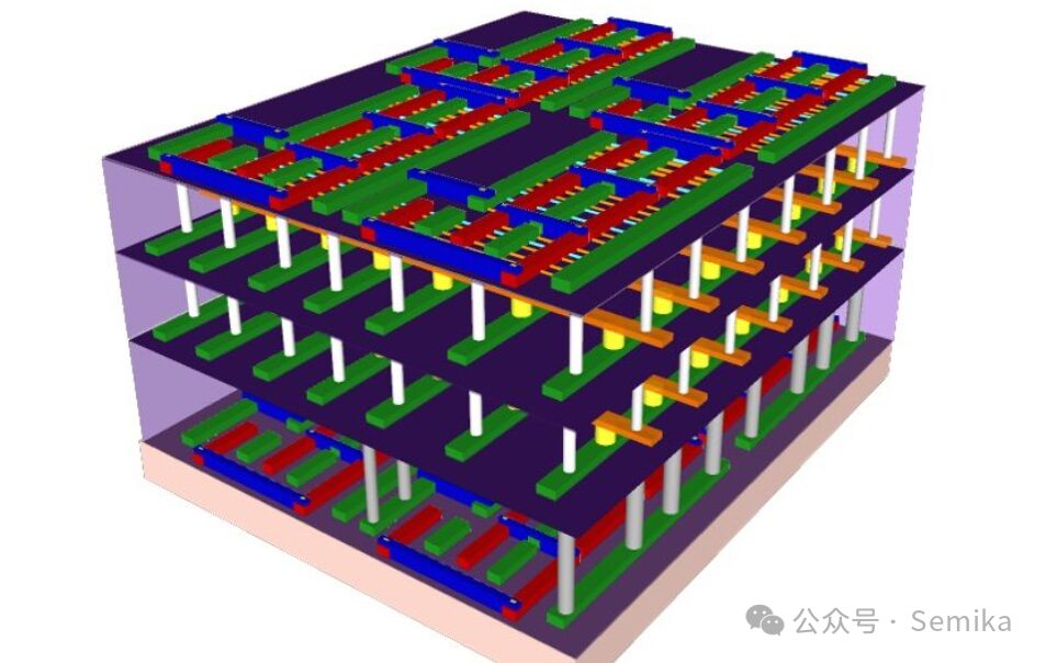
Lithography technology is a key process technology in semiconductors developed based on photography and flat printing technology. In simple terms, integrated circuit manufacturing is to batch produce billions of devices in an area of a few square centimeters, and each device structure is quite complex. The following figure shows an internal structure diagram of a chip that looks difficult to sort out.
This manufacturing density is equivalent to producing tens of millions of such transistors on the cross-sectional area of a hair.
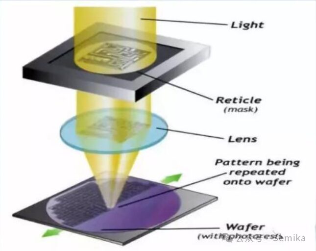
Imagine the photographic process, where light reflected from an object passes through a lens and projects onto a film, causing the photosensitive material on the film to change, thus “transferring” the object to the film; this is an imaging process.
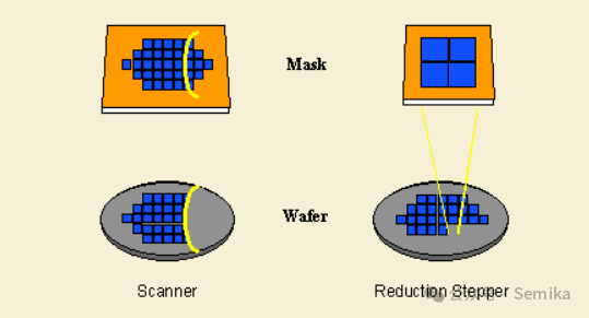
Lithography is similar. As shown in the figure below, the light emitted from a light source shines on the mask, and the outgoing light carries the graphic information from the mask.
Where there are graphics, light can pass through; where there are no graphics, the light is blocked. This way, a graphic structure can be left on the silicon wafer (quartz).
The light that carries the graphic information of the mask shines on the substrate coated with photosensitive material (photoresist), and this process is called exposure.
The properties of the photoresist at the illuminated positions will change, allowing it to dissolve in alkaline or acidic solutions; this process is called development.Through exposure and development, the graphics on the mask are transferred to the photoresist, and then through subsequent processes such as etching or thin film deposition, the graphics on the photoresist are transferred to the substrate.
Lithography machines appeared in the 1960s. Early lithography technology was not particularly difficult, as the line width required for lithography at that time was in the micron range. Therefore, lithography machines were very rudimentary; at that time, Intel directly disassembled a 16mm camera lens and could use it. At that time, lithography machines were not considered high-tech equipment and were not much more complex than cameras.
 However, as the number of transistors continued to double, the exposure accuracy rapidly increased from a few microns to less than 0.1 microns, making these rudimentary lithography machines increasingly unable to meet demand, and more and more issues arose. With more transistors, interconnections increased significantly, requiring multiple layers of metal connections, and metal layers needed to be stacked on dielectric layers, requiring different exposed graphics to be wired on dielectric layers and different masks to be repeatedly exposed. Thus, the issue of repeated alignment accuracy became a major problem, akin to building a building where each layer must align perfectly; it cannot be tilted while being built. In integrated circuit technology, this precision requirement is exceptionally high, reaching the nanoscale…
 At this time, lithography machines had transformed from the extremely rudimentary equipment of early times into the most precise and expensive industrial equipment today, integrating cutting-edge technologies from dozens of disciplines including precision optics, lasers, fluid physics, electromagnetism, precision control, mechanical processing, electronic information, electronic circuits, and chemistry. The high-end models of ASML’s lithography machines even sell for over 100 million dollars, comparable to an airplane.
Early lithography machines were called Mask Aligners, meaning mask alignment exposure. Today, the term lithography is more commonly used to refer to lithography machines and lithography processes, and sometimes process engineers simplify it to “litho”. To refer to lithography machines, engineers typically use words that describe the characteristics of the lithography machines to refer to various types of lithography machines. The advantage is that professionals can immediately understand which specific model of lithography machine you are talking about, while the downside is that outsiders may be left confused.
There are many types of lithography machines, but it can sometimes be difficult to categorize them because some classifications are only subcategories under a certain classification. Below are some main types of lithography machines, and a brief description of the main features of each type is provided. The order is arranged in a way that reflects the gradual improvement of technology, helping to understand the lithography technology from shallow to deep.
At this time, lithography machines had transformed from the extremely rudimentary equipment of early times into the most precise and expensive industrial equipment today, integrating cutting-edge technologies from dozens of disciplines including precision optics, lasers, fluid physics, electromagnetism, precision control, mechanical processing, electronic information, electronic circuits, and chemistry. The high-end models of ASML’s lithography machines even sell for over 100 million dollars, comparable to an airplane.
Early lithography machines were called Mask Aligners, meaning mask alignment exposure. Today, the term lithography is more commonly used to refer to lithography machines and lithography processes, and sometimes process engineers simplify it to “litho”. To refer to lithography machines, engineers typically use words that describe the characteristics of the lithography machines to refer to various types of lithography machines. The advantage is that professionals can immediately understand which specific model of lithography machine you are talking about, while the downside is that outsiders may be left confused.
There are many types of lithography machines, but it can sometimes be difficult to categorize them because some classifications are only subcategories under a certain classification. Below are some main types of lithography machines, and a brief description of the main features of each type is provided. The order is arranged in a way that reflects the gradual improvement of technology, helping to understand the lithography technology from shallow to deep.
-
For example, Exposure Mask Aligner
-
-
-
-
-
DUV/EUV Lithography Machines
Next, we will introduce detailed information about each type of lithography machine.
2.1 Exposure Mask Aligner
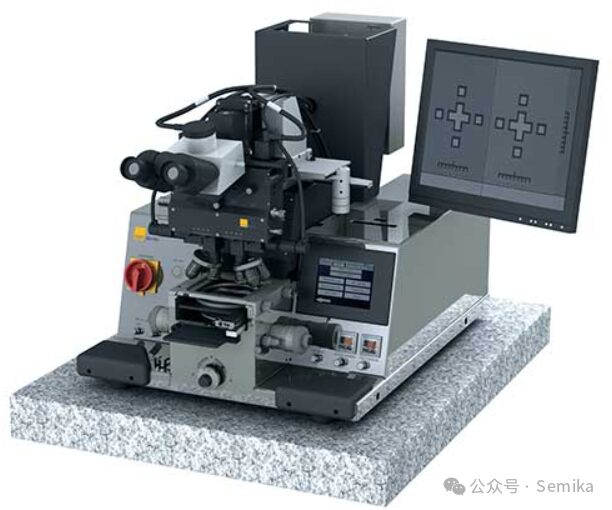
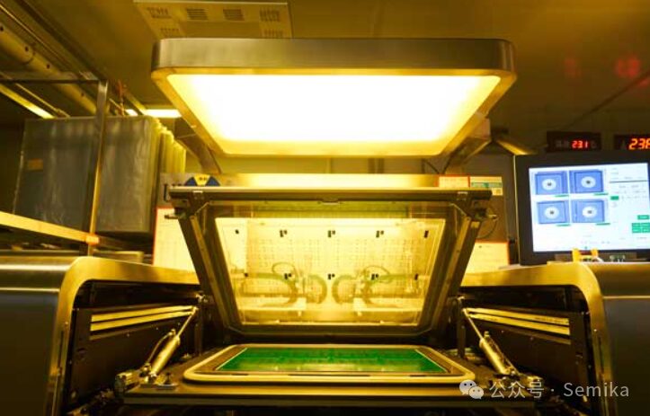
The exposure Mask Aligner is the most direct application of lithography. The simplest mask alignment exposure can be a “manual” device as shown in the figure below, which can achieve mask alignment through a microscope and manual adjustment, followed by exposure for lithography functionality.
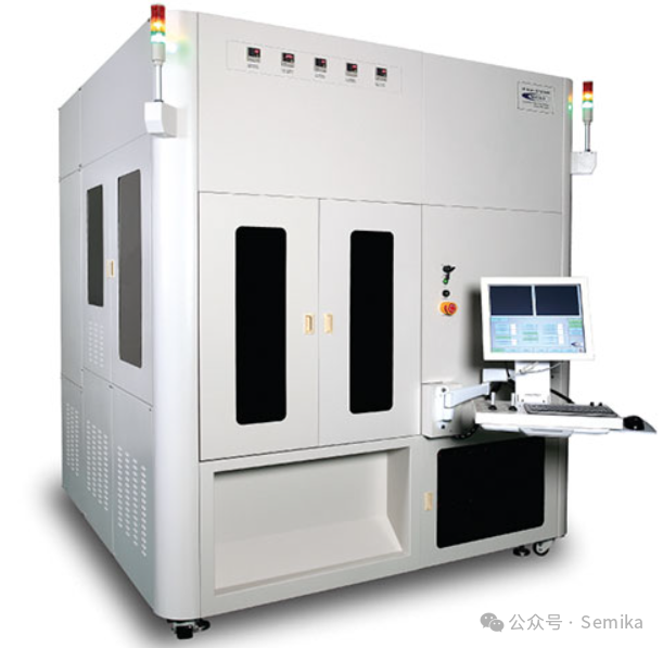
However, the mask alignment exposure machine that can achieve automatic production is much more complex. As shown in the figure below:
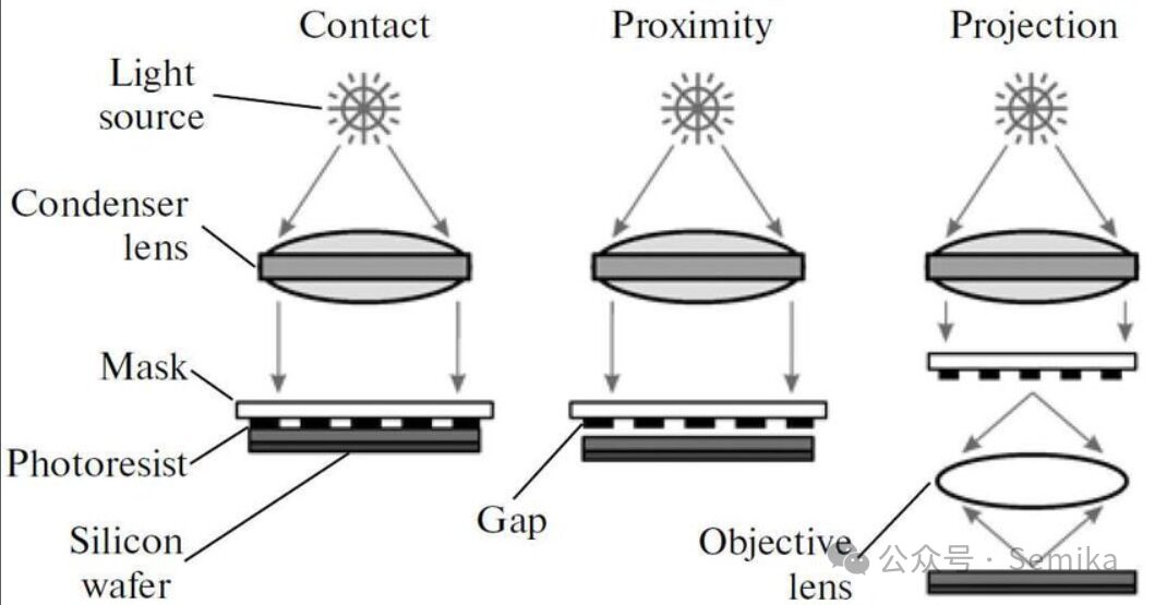
2.2 Contact Photolithography
Contact lithography uses a mask aligner for lithography. The mask aligner has two main tool structures: the mask holder and the wafer chuck. The mask holder is machined to a very flat surface, and the photomask is fixed on this surface by vacuum. The wafer chuck is also machined flat and holds the wafer in the proper position by vacuum. This tool can ensure that the surfaces of the two parts remain parallel to each other during operation. The wafer chuck can move upward to the mask holder to contact the mask with variable force. The surface position of the wafer chuck can also be adjusted to be as close as possible to the mask plane for optimal results; this is called wedge error compensation. Once the wafer and mask are in position, exposure can be performed by opening the shutter on the lamp housing. Inside the lamp housing is a mercury arc lamp and related optical elements that allow a selected controllable ultraviolet band to expose the mask and wafer.
The figure below vividly illustrates three different Mask Align methods: Contact, Proximity, and Projection. Of course, these methods each have significant advantages and disadvantages, as well as their own suitable application fields.
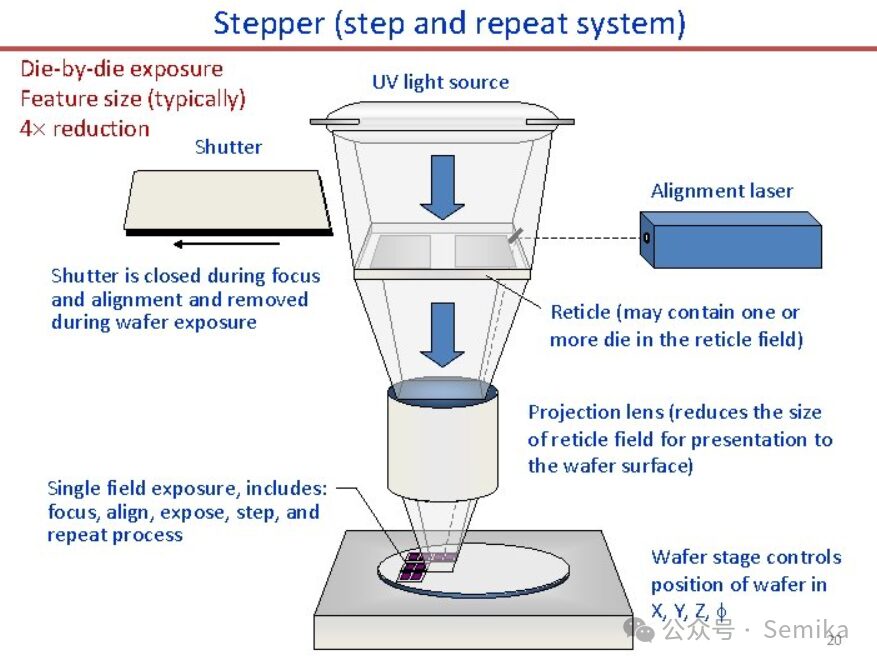
Stepper lithography is designed for smaller and finer chips, adjusting the position of the wafer in a progressive manner and exposing multiple times on a single wafer, also known as a Step and Repeat System.
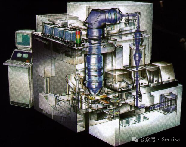
The structure of a stepper lithography machine is quite complex, as shown in the figure below:
2.4 Scanner Photolithography
Projection lithography tools fall into two main categories – scanner and step-and-repeat systems. Scanning projection printing was pioneered by Perkin-Elmer, using reflective optics (i.e., mirrors instead of lenses). When the mask and wafer are moved simultaneously by a slit, light is projected from the slit on the mask to the wafer. The exposure dose is determined by the intensity of the light, the width of the slit, and the speed of scanning the wafer. These early scanning systems used polychromatic light from a mercury arc lamp and were 1:1, meaning the mask and image sizes were equal. The step-and-repeat camera (referred to as the stepper) exposes a rectangular portion of the wafer at a time (called the image field), which can be either 1:1 or reduced. These systems use refractive optics (i.e., lenses) and are usually quasi-monochromatic. Both types of systems can achieve high-resolution imaging, although the highest resolution requires image restoration.
 By the mid-1970s, scanners replaced proximity printing for devices smaller than 4 to 5 μm. By the early 1980s, as device designs pushed below 2 μm, steppers began to dominate. As the minimum feature size reached the 250 nanometer level, steppers continued to dominate photolithography throughout the 1990s. However, by the early 1990s, Perkin-Elmer’s successor SVG Lithography introduced a hybrid step-and-scan approach. The step-and-scan method uses a small portion of the normal step field (e.g., 25mm x 8mm) and then scans that field in one direction to expose the entire 4x reduced mask. The wafer is then moved to a new position, and the scan is repeated. The smaller imaging field simplifies the design and manufacture of lenses but comes at the cost of a more complex aperture and wafer stage. The step-and-scan technology is the preferred technology for manufacturing below 250nm today.
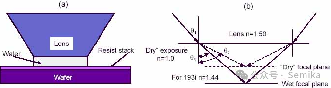
2.5 Immersion Lithography
Immersion lithography is a lithography enhancement technology that replaces the usual air gap between the final lens element and the photoresist surface with a liquid medium that has a refractive index greater than 1. The smaller wavelength in the liquid allows imaging of smaller features, with water currently being used as the liquid. The figure below shows a schematic of the final lens and wafer.
The immersion technology was first introduced by Carl Zeiss in the 1980s to improve the resolution of optical microscopes. In the 1980s, immersion technology was introduced into modern lithography technology. Since 2002, immersion lithography has developed at an incredible pace.
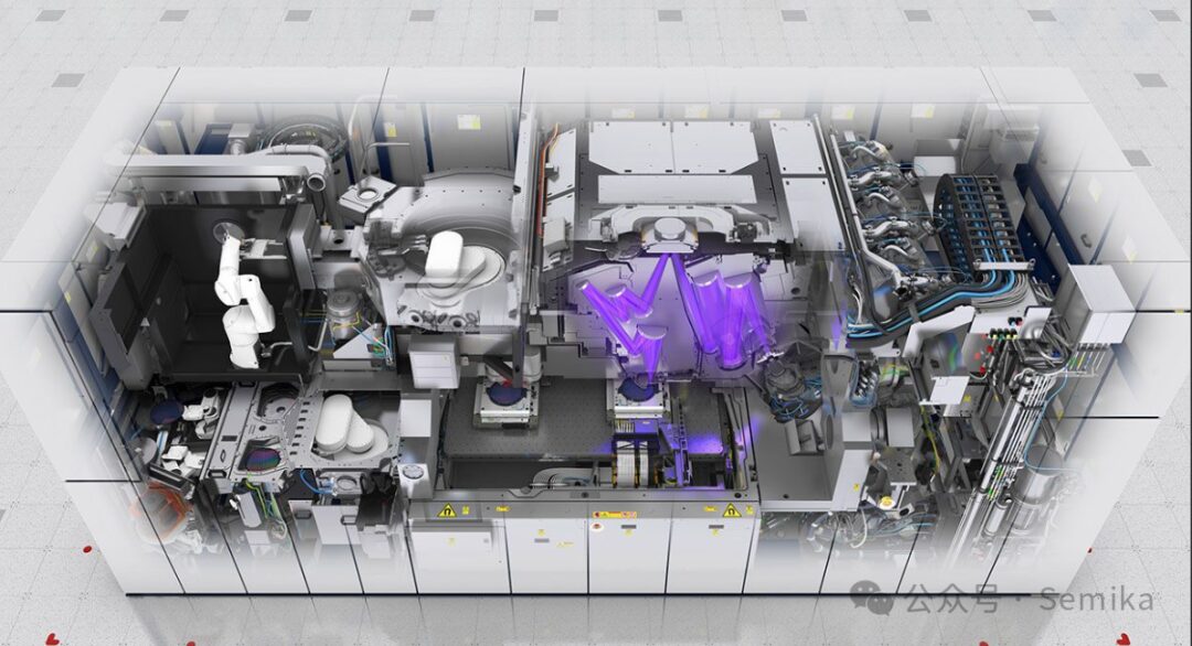
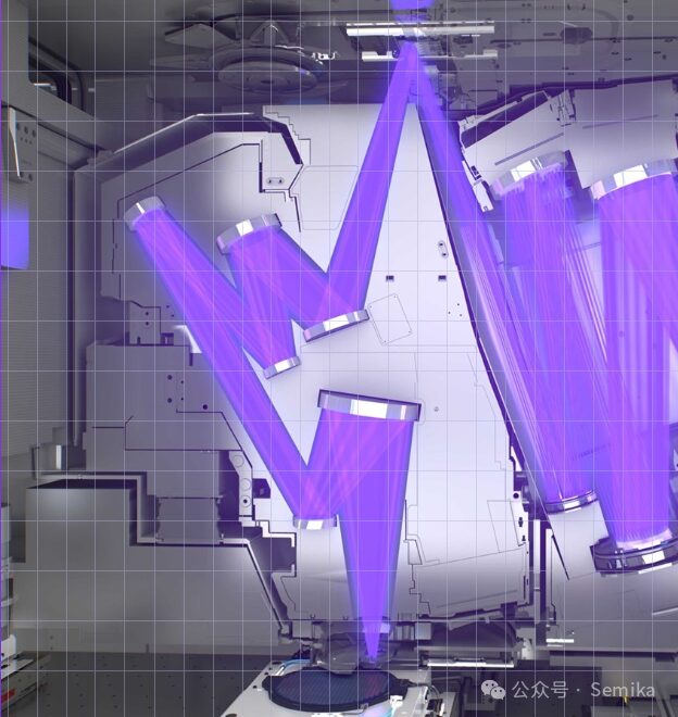
2.6 DUV/EUV Lithography Machines
Resolution is the minimum feature that can be printed under appropriate control, and it has two basic limitations: the minimum image that can be projected onto the wafer, and the resolution capability of the photoresist utilizing that image. In projection imaging, resolution is determined by the wavelength (λ) of the imaging light and the numerical aperture (NA) of the projection lens according to Rayleigh’s criterion.
Lithography systems have evolved from blue wavelengths (436nm) to ultraviolet (UV: UltraViolet, 365nm), to deep ultraviolet (DUV: Deep UltraViolet, 248nm), and now to the mainstream high-resolution wavelength of 193nm. With the development of projection tools and other technologies, DUV technology can produce features smaller than 100 nanometers. In recent years, using overlay offset technology, DUV technology has continuously improved, with production capabilities decreasing to 50nm, 28nm, and even 7nm.
Extreme ultraviolet lithography technology is an x-ray technology with a wavelength of 13.5nm. Today’s EUV scanners can achieve resolutions as low as 22nm half-pitch. In the system, the EUV light source generates plasma using high-power lasers, which in turn helps emit short-wavelength light in a vacuum chamber.
EUV was initially planned to be produced at the 45/40nm process node. However, to achieve sufficient production capacity, the technology underwent multiple upgrades and modifications, delaying shipment times. At the same time, to avoid using the offset overlay pattern technology equipment of the 193nm immersion method, the EUV system only began shipping at the 7nm technology node.
At 5nm, even with EUV, overlay offset pattern technology needs to be applied to critical layers. Although it requires more expensive steps, pattern offset overlap means that the spacing of features can be smaller. Today, 2nm has already started production, all thanks to EUV technology.
By the mid-1970s, scanners replaced proximity printing for devices smaller than 4 to 5 μm. By the early 1980s, as device designs pushed below 2 μm, steppers began to dominate. As the minimum feature size reached the 250 nanometer level, steppers continued to dominate photolithography throughout the 1990s. However, by the early 1990s, Perkin-Elmer’s successor SVG Lithography introduced a hybrid step-and-scan approach. The step-and-scan method uses a small portion of the normal step field (e.g., 25mm x 8mm) and then scans that field in one direction to expose the entire 4x reduced mask. The wafer is then moved to a new position, and the scan is repeated. The smaller imaging field simplifies the design and manufacture of lenses but comes at the cost of a more complex aperture and wafer stage. The step-and-scan technology is the preferred technology for manufacturing below 250nm today.
2.5 Immersion Lithography
Immersion lithography is a lithography enhancement technology that replaces the usual air gap between the final lens element and the photoresist surface with a liquid medium that has a refractive index greater than 1. The smaller wavelength in the liquid allows imaging of smaller features, with water currently being used as the liquid. The figure below shows a schematic of the final lens and wafer.
The immersion technology was first introduced by Carl Zeiss in the 1980s to improve the resolution of optical microscopes. In the 1980s, immersion technology was introduced into modern lithography technology. Since 2002, immersion lithography has developed at an incredible pace.
2.6 DUV/EUV Lithography Machines
Resolution is the minimum feature that can be printed under appropriate control, and it has two basic limitations: the minimum image that can be projected onto the wafer, and the resolution capability of the photoresist utilizing that image. In projection imaging, resolution is determined by the wavelength (λ) of the imaging light and the numerical aperture (NA) of the projection lens according to Rayleigh’s criterion.
Lithography systems have evolved from blue wavelengths (436nm) to ultraviolet (UV: UltraViolet, 365nm), to deep ultraviolet (DUV: Deep UltraViolet, 248nm), and now to the mainstream high-resolution wavelength of 193nm. With the development of projection tools and other technologies, DUV technology can produce features smaller than 100 nanometers. In recent years, using overlay offset technology, DUV technology has continuously improved, with production capabilities decreasing to 50nm, 28nm, and even 7nm.
Extreme ultraviolet lithography technology is an x-ray technology with a wavelength of 13.5nm. Today’s EUV scanners can achieve resolutions as low as 22nm half-pitch. In the system, the EUV light source generates plasma using high-power lasers, which in turn helps emit short-wavelength light in a vacuum chamber.
EUV was initially planned to be produced at the 45/40nm process node. However, to achieve sufficient production capacity, the technology underwent multiple upgrades and modifications, delaying shipment times. At the same time, to avoid using the offset overlay pattern technology equipment of the 193nm immersion method, the EUV system only began shipping at the 7nm technology node.
At 5nm, even with EUV, overlay offset pattern technology needs to be applied to critical layers. Although it requires more expensive steps, pattern offset overlap means that the spacing of features can be smaller. Today, 2nm has already started production, all thanks to EUV technology.
END
This content is reprinted and only represents the author’s views
It does not represent the position of the Semiconductor Research Institute of the Chinese Academy of Sciences
Editor: March
Editor-in-chief: Mu Xin
Submission Email: [email protected]
1. The Semiconductor Institute has made progress in research on bionic covering neuron models and learning methods
2. The Semiconductor Institute has made important progress in inverted structure perovskite solar cells
3. Why is copper used as interconnect metal for chips?
4. What exactly is 7nm for chips?
5. Silicon-based integrated optical quantum chip technology
6. How anomalous is the quantum anomalous Hall effect? It may bring the next revolution in information technology!