Documenting an Issue Related to ALTERA Device JTAG
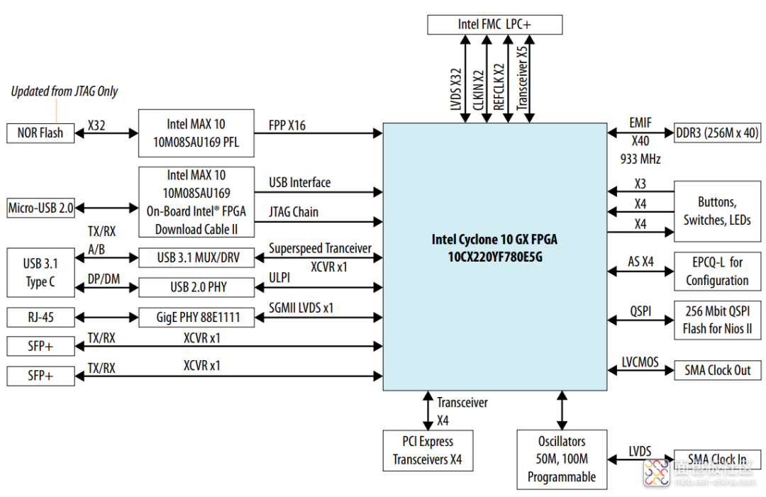
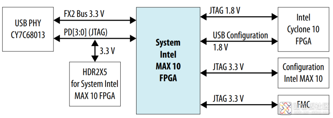
While reviewing previous blog posts, I found several published years ago related to JTAG, specifically: the first one discusses connecting multiple devices on a single JTAG chain: https://mbb.eet-china.com/blog/1010859-213144.html. The second one involves an interesting issue encountered during automatic detection (AUTO Detect) via JTAG interface with the download cable: https://mbb.eet-china.com/blog/1010859-213137.html. This entry also documents an issue related to the JTAG of ALTERA devices, specifically concerning the Cyclone 10 GX series and MAX10 series sharing a single JTAG chain. The problem arose when accessing the JTAG interface via USB Blaster, where automatic detection failed and access was impossible. This issue is quite troublesome; if JTAG cannot be accessed, it means the entire board might be scrapped, which is serious. Is this a hardware design issue, a hardware configuration issue, or something else? A detailed check of the hardware circuit design and the board’s power supply left us all at a loss. For those of us with some FPGA design experience, it felt like a ‘boat capsizing in the gutter.’ A simple JTAG issue took several days to investigate. Although we did not resolve the problem, we could confirm that the hardware design and the configuration mode selection for the CPLD and FPGA were not problematic. So, what could be the cause of the issue? The hardware design reference for this board is based on the ALTERA (now Intel) C10 GX series PCIe development board, which also shares a JTAG chain with M10 and C10GX. The only difference is that the development board has 2 M10 devices and 1 C10GX device, while our board has 1 M10 and 1 C10GX device. The extra M10 is used to implement the USB Blaster downloader function, which is unnecessary for users who can use an external download cable, and generally, users are not familiar with the complete implementation logic of USB Blaster. Since we ruled out hardware design issues, the only remaining concern is that the Cyclone 10 GX series has a power-up requirement different from previous series devices (I am unsure if other 10th generation products have similar requirements). Specifically, the power supply voltages for the FPGA must follow a specific power-up sequence, and the extra M10 device controls the order of power-up voltages. According to the C10GX device manual and related documentation, the power supply voltages for C10GX can be divided into 4 groups, with group 1 powered first, followed by group 2, group 3, and group 4, each with different priorities for power-up. (The power-up sequence requirement will be discussed later). Since the M10 and C10GX are on the same JTAG chain and cannot be successfully accessed, the M10’s program cannot be downloaded, and thus it cannot control the power-up sequence for the C10GX, rendering the C10GX unable to power up successfully. We analyzed whether this was the reason for the instability of the JTAG chain, leading to JTAG access failure. Fortunately, when we discussed this power-up sequence initially, we added an extra controller, allowing the ARM program on the board to participate in control; this was intended as a backup solution. Since the M10 CPLD could not complete the control, we decided to promote this backup solution. After ARM took over control, all power chips on the board entered the ‘ENABLE’ state. It is important to note that when the previous power-up controller failed, it was not the M10’s power supply that failed, but rather the C10GX’s power supply. Our initial intention was to configure the M10 program under the condition of C10GX’s power supply failure, after which the M10 would control the power-up sequence for the C10GX. Now that this control is managed by ARM, all power supplies on the board are operational after power-up. Unfortunately, even so, JTAG was still inaccessible. By this time, nearly a week had passed, and the issue persisted. One day, when a colleague measured the JTAG power supply during AUTO Detect, an anomaly was discovered; we had chosen 1.8V for the JTAG power supply, i.e., VCCPGM=1.8V. The anomaly manifested as VCCPGM being pulled up to over 1.9V after AUTO Detect. In fact, this issue had existed previously, but we had overlooked it, thinking it was an LDO power supply anomaly, and we even tried replacing the voltage regulator resistor and the LDO chip. Now it seems the root of the problem lies with the external USB Blaster download cable. We suddenly remembered that all the USB Blaster cables we had on hand were purchased over a decade ago, and at that time, these cables only supported 3.3V or 2.5V voltages. Thus, when connecting such cables, the automatic detection raised VCCPGM from 1.8V. Before starting this board’s hardware design, we had validated it on the C10GX PCIe development board and had successfully accessed the Cyclone 10GX device using our ‘old’ download cable. Why couldn’t we access our board? Hence, we went back to compare and investigate the original development board schematics and related materials to uncover the reason.