
In the past year, a trend contrary to Moore’s Law has emerged in a certain integrated circuit market – chip prices have increased! According to Moore’s Law, each chip should depreciate by half after 18 months. This market is the memory market, more precisely – DRAM memory. Over the past year, DRAM prices have risen by more than 100%, far exceeding that of M2 hard currency.

There are many types of memory, commonly including ROM (Read-Only Memory), RAM (Read-Write Memory), and a type often overlooked, CAM (you can Google it). Currently, most mainstream memory is RAM, which can be further divided into two types based on their principles – volatile (Volatile) and non-volatile (Non-Volatile, known as non-volatile memory by our compatriots across the strait, which sounds a bit tongue-twisting~). The difference lies in whether data is retained after power loss. Volatile memory includes SRAM/DRAM, primarily used for cache and memory sticks. Non-volatile memory mainly includes hard drives (Hard Disk Drive, HDD) and Flash, used in our USB drives, SD cards, and SSDs.
In this episode of Silicon Talk, we will discuss the past and present of RAM.
The Ancestor That Even Intel Must Respect
The first DRAM chip in human history was invented by Intel, yet almost everyone has forgotten that Intel started as a memory company. This is because Intel, along with contemporaries like TI and Motorola, was defeated by the ancestor of DRAM – the Mostek MK4096P.
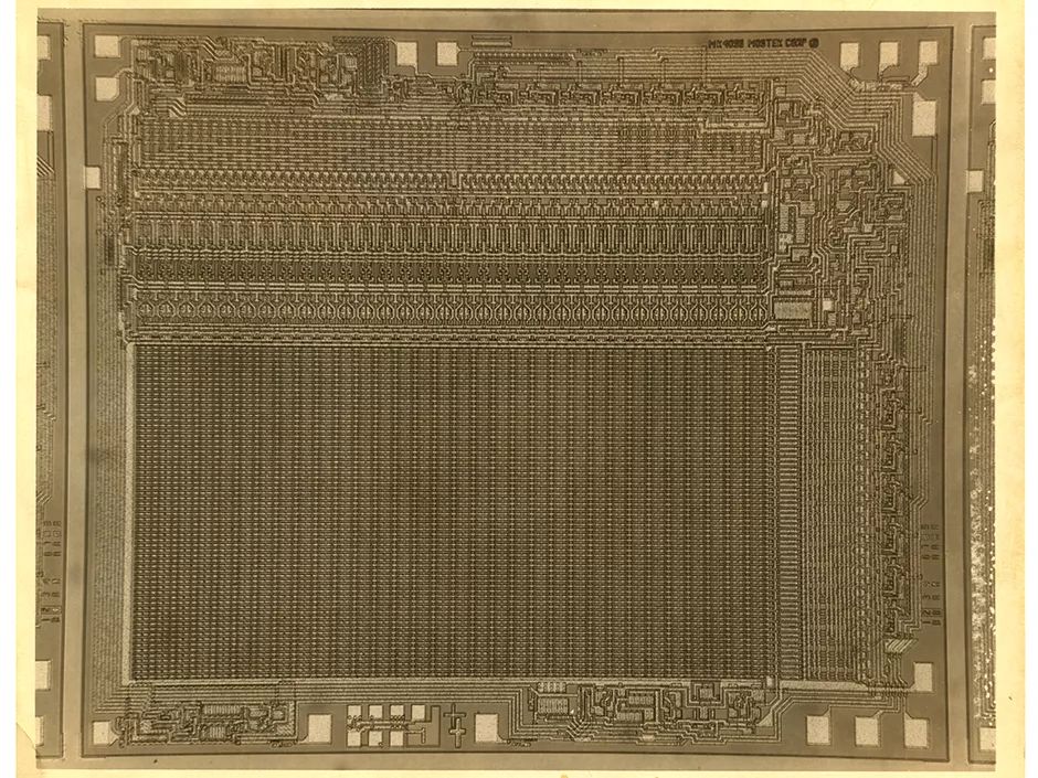
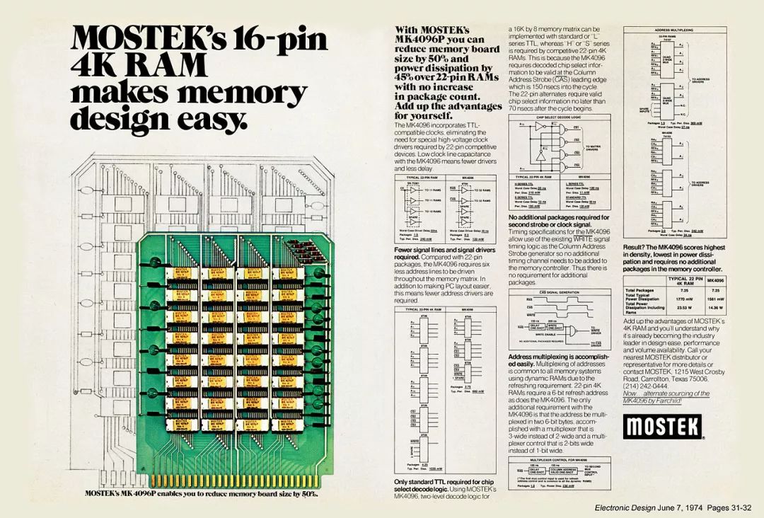
The reason is that for the same size DRAM, they only had 16 pins, while other products of the same era had 22 pins. In an era dominated by DIP packaging, reusing the pins for transmitting row and column index provided a critical advantage in system-level design, known as address multiplexing technology. Even today, this technology is still used in DRAM products. Looking at the prehistoric memory sticks in the image below, you can see the difference in PCB size between the 22-pin and 16-pin memory sticks; the 16-pin design effectively reduced the physical area of the memory card by 50%. No wonder that within a year of the MK4096P’s release, there were no more 22-pin DRAMs.
Additionally, let me share a little story about the semiconductor business – Intel was once the dominant player in DRAM, holding an 85% market share in 1974. However, ten years later, Intel’s DRAM market share plummeted to only 1.3%. It was in this year that the famous Gordon Moore (the Moore of Moore’s Law) and Andy Grove decided that Intel would completely exit the DRAM market, prioritizing CPU development and production (so for the first 20 years, weren’t they prioritizing CPUs?). Of course, Intel was not only defeated by MOSTEK, but also by our neighbor, Japan, which relied on price wars, something Asians excel at. A few years later, MOSTEK, which once surpassed Intel and held an 85% market share, was acquired and eventually became part of STM.
It cannot be denied that Japan’s memory industry in the 1980s was shining brightly. (Recently, there have been many articles online criticizing how many awards Japanese people have won, but looking back at the 1980s, one must admit that Japan was indeed on a complete roll.) Not only did they excel in DRAM, but they also invented something remarkable – NAND flash. Although SRAM/DRAM had emerged in the 60s and 70s, they could not replace the traditional magnetic medium’s power-off storage method. Even ten years ago (in 2008), most PCs still used magnetic storage as their primary hard disk mechanism. However, today, from smartphones to PCs, we seem to have completely bid farewell to HDDs. This is all thanks to the NAND Flash invented by Toshiba –
The concept of NAND flash was proposed in 1984 at the IEDM (International Electron Devices Meeting), but the first NAND flash product was not released until 1989. During this time, it is said that Intel also “borrowed” the concept of NAND flash to propose NOR flash.
At this point, let’s discuss the differences between NAND and NOR flash. From the image below, it is clear that the gate sources and drains of NAND flash are continuous and connected in a cascode configuration, making each cell’s area much smaller, whereas the sources and drains of NOR are separate, occupying more area. Additionally, each NOR cell is connected to the bit line, allowing for random reads. In contrast, a NAND cell only connects the topmost cell to the bit line, thus only allowing sequential block reads. Therefore, NAND often has a larger capacity but cannot be read randomly, while NOR, though limited in capacity, allows for easier reading.
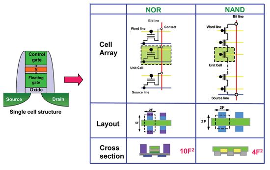
Figure 1: Comparison of NAND and NOR flash
High Walls – The Reincarnation of Moore’s Law
In fact, both DRAM and NAND flash have long collided with the iron wall of the end of Moore’s Law, unbeknownst to us for the past ten years. This is particularly serious for NAND flash, as flash erasing requires high voltage. In processes below 16nm, high voltage can easily cause crosstalk with nearby gates, leading to erroneous writes. So, will memory just watch helplessly as the density limit approaches?
Looking back from now, we suddenly realize that over the past decade, both DRAM and NAND flash have been moving further down the path of 3D integration. In the field of NAND flash, memory giants have proposed various stacking methods for flash, as shown in the image below.
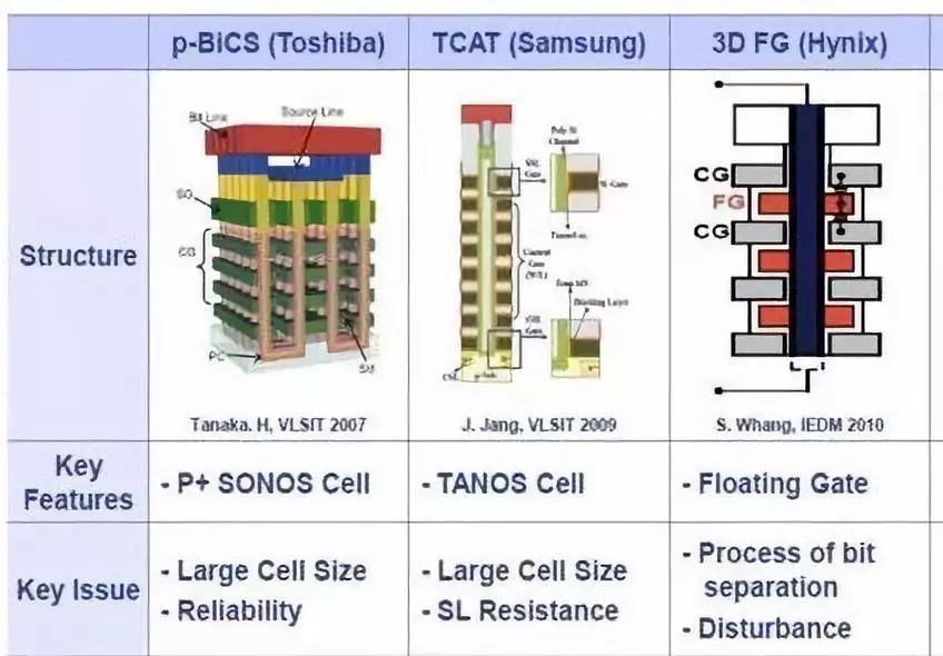
3D NAND flash is not just a stacking of multiple chips; it directly constructs NAND flash (as referenced in Figure 1) vertically. Thus, the number of transistors in a given area is equivalent to the number of stacked layers. Therefore, the expectation of reducing transistor area in Moore’s Law has shifted to increasing the number of stacking layers. Currently, it is reported that NAND flash with 64 layers and even higher has already been mass-produced.
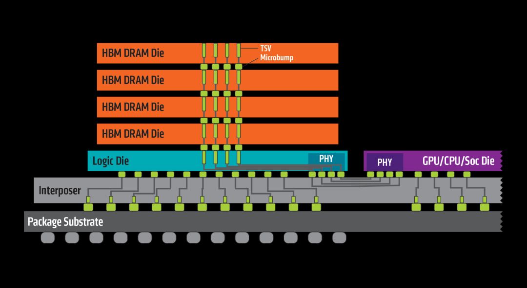
The same story is happening with DRAM, though with different technology. Silicon Talk introduced the HBM DRAM solution a long time ago (those years, we chased Moore’s Law together (Part 2)). This is also one of the mainstream solutions for GPU/AI processors today. HBM DRAM links multiple DRAM chips vertically through TSV technology, enabling communication with CPUs/GPUs/AIs through a base interface chip. 3D/2.5D/2.1D packaging shortens the access latency of DRAM, further enhancing system performance. This technology has already been mass-produced in AMD/NVidia’s new GPUs.
In summary, whether it is NAND flash or DRAM, both are moving towards 3D integration, increasing the number of transistors per unit area by building taller structures. Additionally, it is worth mentioning that as the access speed of memory has become a major bottleneck for many systems, memory interface design has also made significant advances. NAND flash has transitioned from traditional SATA to PCIe 3.0, while DRAM’s DDR interfaces have developed over five standards based on different application scenarios.

The Ultimate Fantasy:
High-Speed Non-Volatile Embedded Memory?
In fact, apart from SRAM/DRAM, many types of RAM have emerged in the past ten years, such as RRAM/MRAM/PRAM/… However, as of today, most have not been commercially adopted on a large scale, but I believe that in the near future, these new devices may experience explosive growth. First, let’s summarize the common characteristics of these RAMs – they all claim to be non-volatile storage, but with read/write speeds that rival SRAM and densities that compete with NAND flash/DRAM.
Let’s take a look at the recently popular STT-MRAM (Spin Transfer Torque Magnetic RAM), which utilizes electron spin to store 0/1. In the image on the left, there is a Magnetic Tunnel Junction (MTJ). The spin direction of the electrons in the upper layer (storage/free) can be changed by the write current, while the spin direction of the lower layer (reference/pin) is fixed. When both directions are the same, it stores 0; when different, it stores 1. The write process of this memory involves changing the spin direction using STT current.
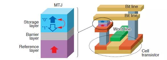
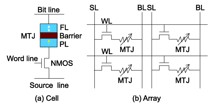
Although theoretically the insulating layer should not conduct electricity, tunneling effects can create resistance characteristics (omitting a thousand formulas here, quantum mechanics flies by…). In the circuit, the same or different spin directions will lead to a huge difference in access resistance (high resistance in reverse, low resistance in the same direction), allowing the resistance of the selected word line’s MTJ to be checked by precharging the bit line during reading. The array structure is shown in the image below.
Besides STT-MRAM, there is another star called ReRAM, where Re stands for resistive. From a circuit principle perspective, ReRAM and MRAM are quite similar, with a variable resistor connected to the bit line, whose resistance represents the stored value. This resistance is achieved through a special medium between the top electrode and bottom electrode, often a metal oxide. When a positive pulse passes from TE to BE (as shown in the set state below), it presents a low resistance on the bit line, while applying a negative pulse (as shown in the reset state) results in high resistance. The reading method is similar to that of MRAM.
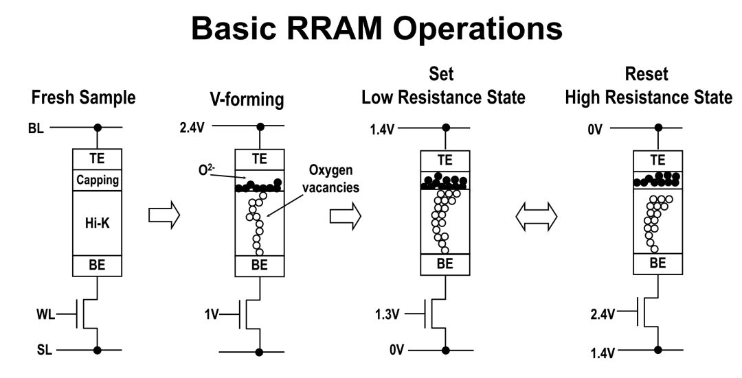
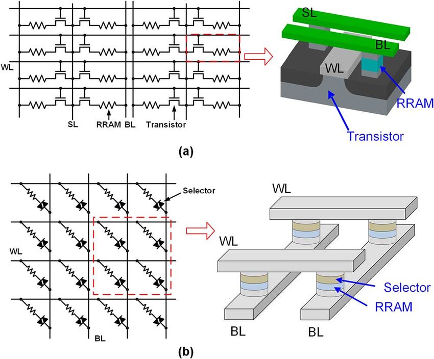
In recent years, RRAM has undergone further upgrades, implementing multi-layer crossbar/cross point structures. This replaces the original NMOS transistor with a selector, which operates similarly to a diode. By properly controlling the voltage on the WL/BL, various states such as read/set/reset can be achieved. This technology can allow RRAM to stack (though there are still some issues with IR drop and sneak current), with densities comparable to NAND flash. Moreover, the read/write speed of ReRAM is over 1000 times that of standard NAND flash, making it a perfect device for the new era.
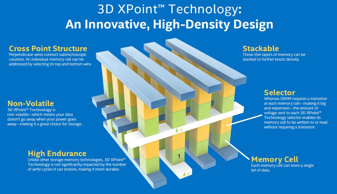
All major companies, including TSMC, Samsung, and Intel, have heavily invested in these new era memories. Intel refers to its 3D crossbar RRAM technology as Optane Technology/3D Xpoint, which has been in preparation for a long time.
In addition to achieving fast read/write and new non-volatile mechanisms, new memory types also strive for compatibility with existing CMOS processes. TSMC has provided embedded MRAM (eMRAM) IP at 22nm and will offer eRRAM IP next year. Once these two (especially eRRAM) achieve compatibility with CMOS processes, they are considered core technologies for true brain-like processors and in-memory computing.
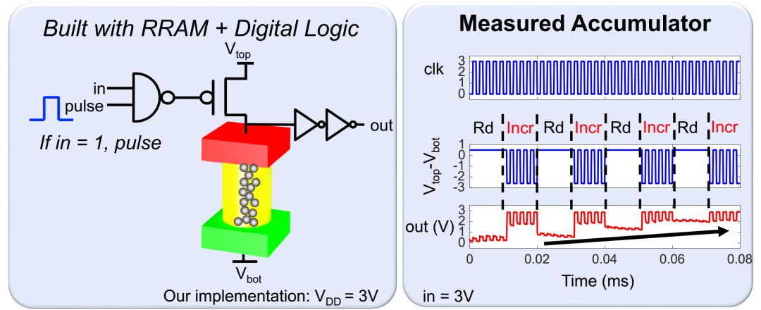
This is a circuit structure proposed by MIT academic star Max Shulaker’s group, which recently received $61 million in funding from DARPA, to implement RRAM as a simulated synapse (accumulation). When positive pulses are continually applied to the RAM, the resistance increases, allowing it to function as an accumulator (ISSCC 2018 31.3) and also simulate the learning mode of the human brain’s STDP – continuous stimulation enhances the connection, while lack of stimulation reduces it.

However, the core of these circuit implementations must be compatible with CMOS logic processes. With one of his former bosses, Philip Wong, moving to TSMC as CTO, we have reason to believe that the day when commercial CMOS processes can be compatible with eRRAM is not far off.
In summary, are you ready to allocate more space on your SSD for MRAM/RRAM?
Source: Silicon Talk
Editor: Shi Xiaoqi