Click the “Materials Science and Engineering” above to quickly followA comprehensive, professional WeChat platform for materials science
Compared to traditional liquid crystal display (LCD) screens, Organic Light Emitting Diode (OLED, also known as Organic Electroluminescent Display) screens are widely recognized as the next generation display technology. They not only have advantages such as all-solid-state, lightweight, active light-emitting, high picture quality, and low power consumption but can also be used to explore transparent, rollable, foldable, and curved screen forms that break traditional screen formats. OLED is the future display technology direction that the industry is collectively focused on. However, compared to small and medium-sized OLED screens that use low-temperature polysilicon technology, large-sized OLED screens that apply oxide technology face numerous technical challenges in popularization. Currently, the large-scale application and industrialization of OLED panels are still a long way off due to constraints from key technologies, costs, and low yield rates.
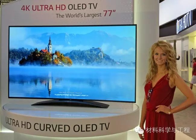
Products using OLED large screens
The panel, organic material coating, and packaging are the three major indicators for the mass production of OLED large screen products. Due to the bottleneck in developing large-sized devices, the low-temperature polysilicon (LTPS) panel process cannot cross the 5.5-generation OLED screen production line. This technology requires the red, green, and blue organic light emitters to be horizontally vapor-deposited on a glass panel. Since a metal mask must be used during vapor deposition, gravity can cause the metal mask to sink and lead to color mixing issues when making large panels, making it unsuitable for achieving large screens and high resolutions. Therefore, amorphous silicon (a-Si) and oxide thin-film transistors (Oxide TFT) panels have become the choices for technological development. However, the former’s electron mobility is too slow, which reduces the dynamic display response speed of OLED panels. As a result, the latter has become the preferred choice for technological development, but progress in this technology has always been slow. The materials and processes for oxide thin-film transistor panels are similar to those of amorphous silicon, so some existing amorphous silicon processing equipment can be used for oxide thin-film transistors.
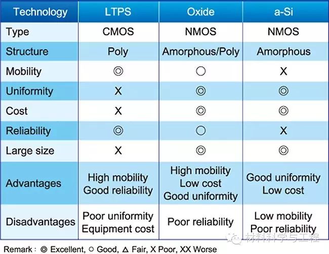
Panel technology comparison table
Common oxide semiconductors, such as indium gallium zinc oxide (InGaZnO), are new materials with electron mobility reaching 10 square centimeters (cm2)/VS, which is tens of times higher than traditional amorphous silicon (<1cm2/VS). Additionally, the amorphous structure can achieve good uniformity in large sizes, suitable for application in large screens, providing high clarity, low energy consumption, and low leakage advantages. However, its reliability issues and difficulties in PMOS manufacturing processes have been ongoing challenges that need improvement. The former is a critical hurdle for mass production commercialization, while the latter can be overcome with compensation circuits.
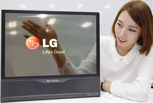
Products using OLED transparent screens
Common structures of oxide thin-film transistor components mainly include coplanar, etched stop layers (Island Stop/Etch Stop Layer, IS/ESL), and back channel etch (Back Channel Etch, BCE). The coplanar structure has a simple process, but the oxide semiconductor layer must climb over the source-drain metal, which can easily lead to electrical characteristics and contact issues, and its reliability is poor. In contrast, back channel etch and etched stop layer structures have advantages in component characteristics and process yield, especially since the back channel etch structure is compatible with standard amorphous silicon structures, making it highly competitive. However, considering reliability, the etched stop layer structure is the most ideal because the etching stop layer can protect the back channel of the component from process-induced characteristic differences, although its complexity leads to yield issues.
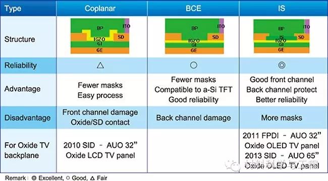
Comparison table of common oxide thin-film transistor component structures
The importance of oxide thin-film transistor technology lies in its compatibility with existing mainstream amorphous silicon equipment for mass production. Due to the material characteristics of oxide thin-film transistors, light and heat can alter electrical characteristics, specifically the threshold voltage shift (Vth Shift), and they can even be applied in photo sensors. Therefore, improving uniformity and reliability will be a significant challenge, as process calibration is quite difficult and sensitive, and the stability requirements of the process are relatively high. Through continuous analysis and improvement with the lab, researchers have developed an entire OLED critical voltage shift value of less than 0.8 volts on the oxide technology trial production line. After panel reliability testing, it was found that the estimated lifespan could exceed 10 years, surpassing traditional amorphous silicon technology and nearing low-temperature polysilicon technology.
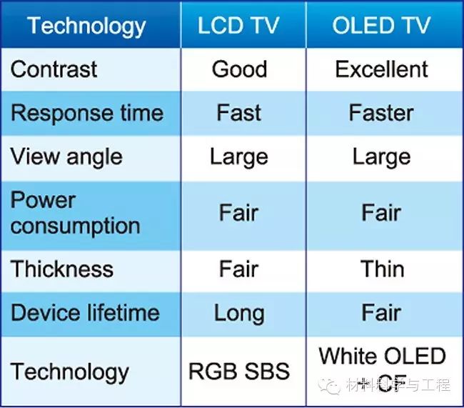
LCD and OLED characteristics comparison table
OLED screens consist of red, green, and blue (R, G, B) pixels, utilizing mainstream organic material coating technology—vapor deposition. This production method requires balancing the placement of red, green, and blue organic materials within each pixel to maintain uniform brightness. As the size of OLED screens increases, production yield rates decrease. Due to the short lifespan of blue organic emitters, to repair their defects, a slightly larger amount of blue OLED organic emitters is deposited, which results in color distortion in the red, green, and blue pixel structures. In addition to issues caused by the design of the vapor deposition tank that lead to poor production efficiency, there is also the dilemma of the difficulty in obtaining vapor deposition equipment suitable for 8-generation OLED screen production lines. In addition to continuing to use the 5.5-generation line to produce OLED screens, laser technology can be used for organic material coating, or oxide panels can be paired with white OLEDs and color filters to extract the three primary colors red, blue, and green, which is closer to the current LCD screen production process. This involves vertically vapor depositing the red, green, and blue organic light emitters on a whole white OLED panel and using color purification technology to convey color information. After coating, a diffusion film is used to achieve an even surface light source. This method does not use a metal mask during organic vapor deposition, so it is not limited by panel size, allowing for uniform organic vapor deposition and achieving color enhancement through the vertical vapor deposition of red, green, and blue organic light emitters, thus effectively resolving the lifespan issue of blue organic light emitters, although its color performance is relatively poor and power consumption is high, but the yield is relatively high and suitable for mass production.
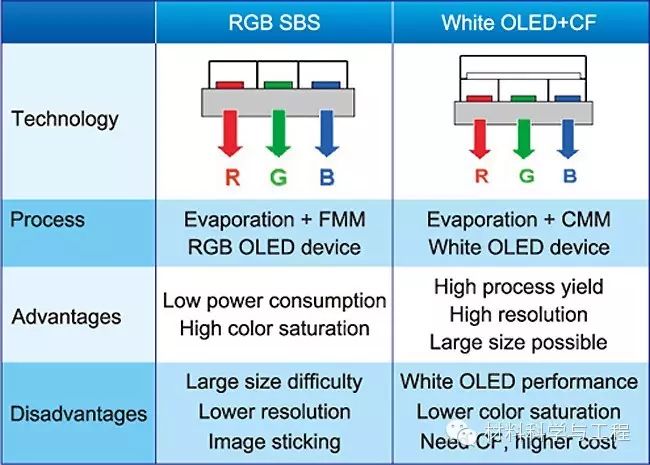
Common full-color OLED technology comparison table
Common full-color OLED technologies mainly include the red, green, and blue pixel arrangement method (RGB-SBS, Side-By-Side) and white OLED + color filter technology. The red, green, and blue pixel arrangement method consists of red, green, and blue pixels emitting light separately, which not only achieves better color saturation but also saves energy, although large-sized vapor deposition (Evaporation) is challenging and requires continuous development.
Although the finely detailed metal mask (Fine Metal Mask, FMM) pixel technology with a relatively difficult process has better color performance and energy efficiency, it immediately faces challenges of scaling up, including the need for fine metal masks and no color mixing requirements, as well as challenges with metal vapor deposition processes exceeding 1000°C. Researchers strictly implement process control, efficiently feedback process parameters, and, with fine divided sheet (Fine Divided Sheet, FDS) technology, have successfully developed non-color mixing technology, achieving a milestone for both front-end oxide thin-film transistors and back-end OLED to be produced as full sheets.
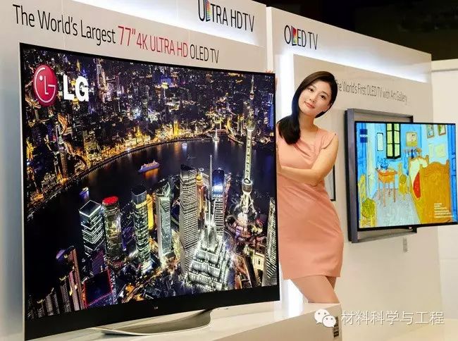
Products using OLED curved screens
Since the tandem OLED structure was published, high-efficiency white OLED has gradually become a reality. With the advancement of materials and component technology, white OLED technology has reached an acceptable level in both the lighting and display fields. However, compared to OLEDs using the red, green, and blue pixel arrangement method, which offers a wide color gamut and high color purity, white OLED components still fall short. Additionally, the composition of white light components requires at least 10 layers of films, and over time, the uniformity of film thickness on each OLED component remains a significant issue that needs to be resolved in metal vapor deposition equipment.

Products using OLED large screens
In recent years, apart from material advancements, the improvement of OLED component technology has been a key factor for the success of the entire OLED industry. The optical thickness design of components is crucial; optimizing the optical thickness allows the colors emitted by organic light-emitting materials to achieve optimal performance, while planning the up or down light-emitting components and strong or weak resonance cavities (Cavity) according to product properties. The OLED components are designed using multiple transmission layers and new blue light-emitting materials, thus achieving high efficiency and good blue color performance on the down light-emitting component in a weak resonance cavity, presenting an 83% color gamut performance in the CIE1931 color coordinates. Additionally, due to the application of multiple transmission layers, the energy recovery on the triplet state of the fluorescent light-emitting layer material has significantly improved the component’s efficiency. Furthermore, the OLED component is equipped with patented OLED pixel compensation circuit technology (OLED Engine), which effectively improves the brightness uniformity caused by the critical voltage shift of oxide thin-film transistors and OLEDs.
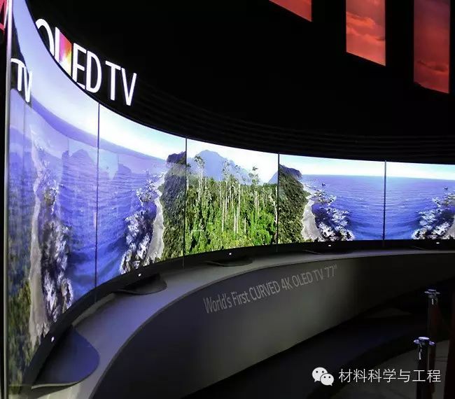
Products using OLED curved screens
To achieve thinner and lower-cost OLED screens, a mass-producible thin film packaging technology must replace traditional glass packaging technology. OLED screens are composed of upper and lower panels. In traditional processes, the upper panel generally uses glass packaging; however, the trend is towards the lightweight, thin, and low-cost thin film packaging technology. Since the low-temperature polysilicon panel process temperature reaches 600°C, the heat resistance of glass panels is poor, thus limiting the thermal resistance of OLED glass panels due to technical constraints. To improve the yield of low-temperature polysilicon panel processes and shorten the mass production time of OLED screens, OLED glass panel companies will produce lotus glass suitable for low-temperature polysilicon high-temperature processes. This glass panel features zero impurities, high flatness, and heat stability to supply some existing 4.5 and 5.5 generation OLED screen production lines.
Currently, organic optoelectronics still has a series of theoretical, technical, and process issues that need to be resolved in terms of materials, efficiency, lifespan, colorization, large size, flexibility, packaging, and production processes. The deficiencies in these areas significantly restrict the industrialization direction of organic optoelectronic functional materials and technologies. Among them, the large-scale application of OLED technology depends on comprehensive advancements in materials, design, and preparation processes, as well as innovations in materials and device structures to improve efficiency, increase stability, and reduce costs.
Source: Tadpole Five-Line Staff
Today’s Editor: Valley Stream