Main reference materials:
Bilibili @ Jiangxie Technology
STM32 Beginner Tutorial – 2023 Edition Detailed Explanation with Chinese Subtitles
Development materials download link: https://pan.baidu.com/s/1h_UjuQKDX9IpP-U1Effbsw?pwd=dspb
Microcontroller kit: STM32F103C8T6 development board microcontroller C6T6 core board experimental board minimum system board kit
Article source file: https://github.com/INKEM/Knowledge_Base
This chapter is the final chapter based on Jiangxie Technology’s STM32 beginner tutorial, marking the end of the STM32 microcontroller series updates. Due to the author’s limited learning time, the presentation of content for readers has not been thoroughly considered. Suggestions from some readers have been noted, but further optimization is not feasible, and I ask for your understanding. Of course, for a more complete learning experience, I still recommend following Jiangxie Technology’s videos for step-by-step practical learning, as purely text and images can be tedious and lack effective presentation. The function of this article is more to help everyone organize the knowledge points from the videos for efficient review and recap.
Regarding further updates on STM32, the author will proceed as time allows. Possible content includes: more module tutorials released by Jiangxie Technology and the author’s planned self-expansion knowledge summary series 【STM32+】, tutorials based on the HAL library development method 【STM32HAL Library】 series, and a comprehensive optimization and expansion of previously updated content in the 【STM32】 Phase II series. However, the author still has more areas of knowledge to learn, and these are currently just lofty ideas that may take years to realize.
Introduction to FLASH
- • The FLASH of the STM32F1 series includes three parts: program memory, system memory, and option bytes. The program memory and option bytes can be erased and programmed through the flash memory interface (peripheral).
- • Uses of reading and writing FLASH
- • Utilize the remaining space in program memory to store user data that is not lost during power-off.
- • Achieve self-updating of the program through in-application programming (IAP).
- • In-Circuit Programming (ICP) is used to update the entire content of the program memory, which can be downloaded via JTAG, SWD protocol, or system bootloader.
- • In-Application Programming (IAP) can use any communication interface supported by the microcontroller to download the program, requiring a custom-designed bootloader, which is not covered in this section.
FLASH Module Organization
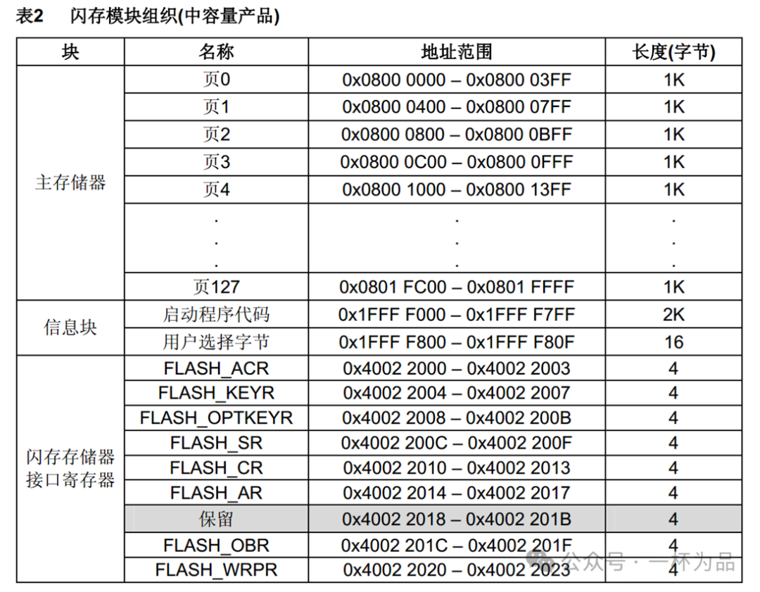
The FLASH module organization is divided into three blocks. The main memory stores the program code and is the largest block (128K in the table, but the C8T6 model only has the first 64K). The information block can be divided into bootloader code and user option bytes, where the bootloader code is factory-written for serial downloading, and the user option bytes store independent parameters. The flash memory interface register is a regular peripheral that does not belong to FLASH, with SRAM as the storage medium, used to control the erasure and programming process of FLASH, while reading FLASH can be done using pointers.
Similar to the W25Q64 flash in SPI communication, the main memory is paginated for better management of FLASH, with erasure and write protection done on a page basis, and its operational characteristics are the same as those of the W25Q64 flash.
Basic Structure of FLASH
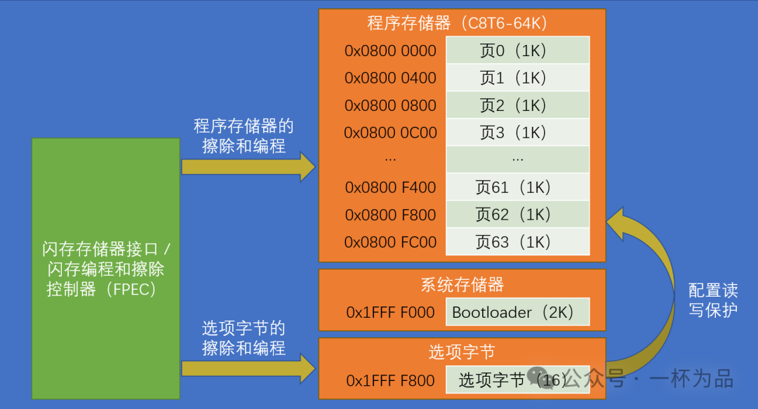
The above figure shows the basic structure of the entire FLASH. The flash memory interface (FPEC) can erase and program the program memory and option bytes, but cannot operate on the system memory. A large portion of the option bytes is used to configure read/write protection for the main program memory, and some configuration functions will be explained later.
FLASH Operations
FLASH Unlocking
The first step in controlling FPEC to erase and program the program memory and option bytes is FLASH unlocking, which is equivalent to write enable for the W25Q64.
- • FPEC has three key values:
- • RDPRT key = 0x000000A5 (to remove read protection in option bytes)
- • KEY1 = 0x45670123
- • KEY2 = 0xCDEF89AB
- • Unlocking:
- • After reset, FPEC is protected and cannot write to FLASH_CR.
- • Write KEY1 to FLASH_KEYR first, then write KEY2 to unlock.
- • An incorrect operation sequence will lock FPEC and FLASH_CR until the next reset.
- • Locking:
- • Set the LOCK bit in FLASH_CR to lock FPEC and FLASH_CR.
- • Locking should be completed as soon as possible after the operation to prevent unexpected situations.
Accessing Memory Using Pointers
Use pointers to read registers at specified addresses:
uint16_t Data = *((__IO uint16_t *)(0x08000000));0x08000000 is the address of the register to be accessed, and the parentheses ensure priority (in case of address calculations). The address is cast to a pointer type of uint16_t, and then the memory pointed to by the pointer is accessed. In STM32, the following macro is defined:
#define __IO volatileAdding volatile before the data type is a safety measure to prevent compiler optimization. Compiler optimization may remove unnecessary complex code, reducing code space and improving runtime efficiency, but in some cases, it may backfire. Volatile should be added when dealing with meaningless increment/decrement variables, multi-threaded variable changes, and reading/writing hardware-related registers.
Use pointers to write to memory at specified addresses:
*((__IO uint16_t *)(0x08000000)) = 0x1234;Program Memory Operations
The following program flowcharts are encapsulated in library functions; understanding the process is sufficient.
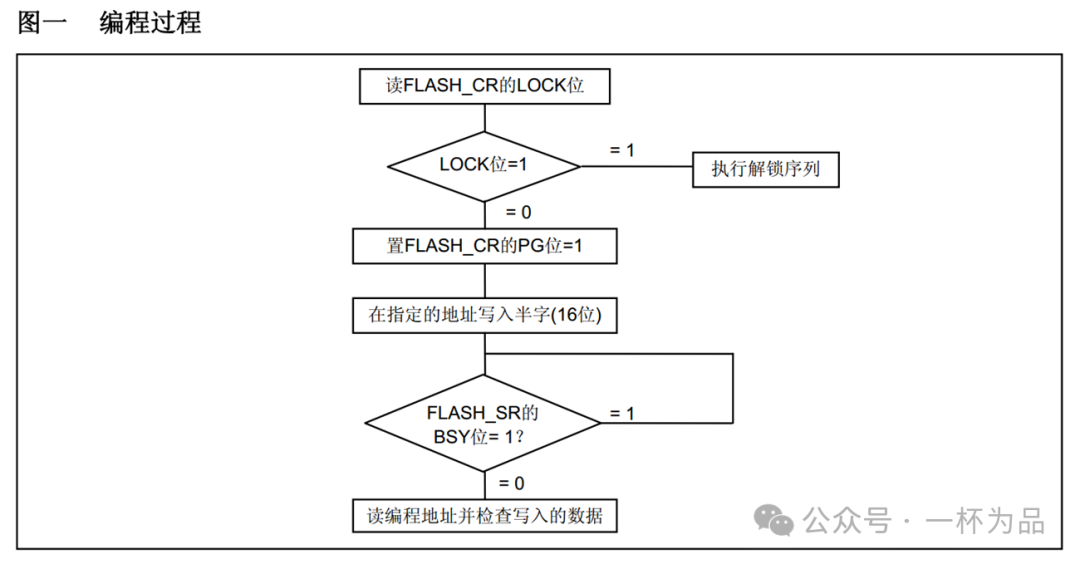
Full Erase of Program Memory
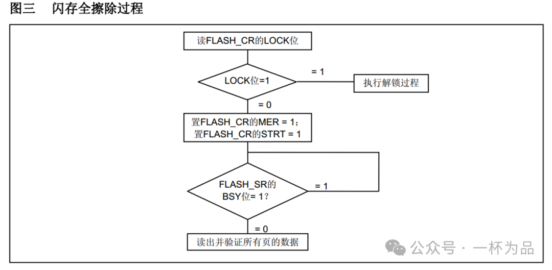
First, read the LOCK bit to check if the chip is locked. If LOCK bit = 1, execute the unlocking process, but in the library function, the unlocking process will be executed regardless of whether it is locked or not. After unlocking, set the MER (Mass Erase) bit of the control register to 1, then set the STRT (Start) bit to 1. Setting STRT to 1 is the trigger condition; once the condition is met, the chip begins to execute the operations corresponding to the control register bits (in this case, a full erase). The erasure process takes time, so after starting, the program must wait and check the BSY (Busy) bit of the status register until BSY bit = 0 to exit the loop. Reading and verifying all page data is the task of the test program, and under normal circumstances, a full erase is considered successful by default.
Page Erase of Program Memory
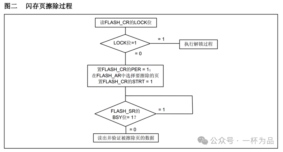
Except for different register configurations, the other program memory operations are generally the same as the full erase process. In page erase, the PER (Page Erase) bit of the control register must be set to 1, then write a page start address in the address register to select the page to be erased, and finally set the STRT bit of the control register to 1.
Programming Program Memory
Before writing to STM32 FLASH, it checks whether the specified address has been erased. If it has not been erased, STM32 will not perform the write operation unless writing all zeros. The write operation sets the PG (Programming) bit of the control register to 1, then uses the pointer to write half-word 16-bit data at the specified address. 32-bit data must be written in two steps, while for 8-bit data, to avoid affecting other data, the best method is to read a page of FLASH into SRAM, write it, then erase a page in FLASH, and write back the entire page of data from SRAM. Writing does not require the trigger condition of the STRT bit.
Option Byte Operations (For Understanding)
Option Bytes
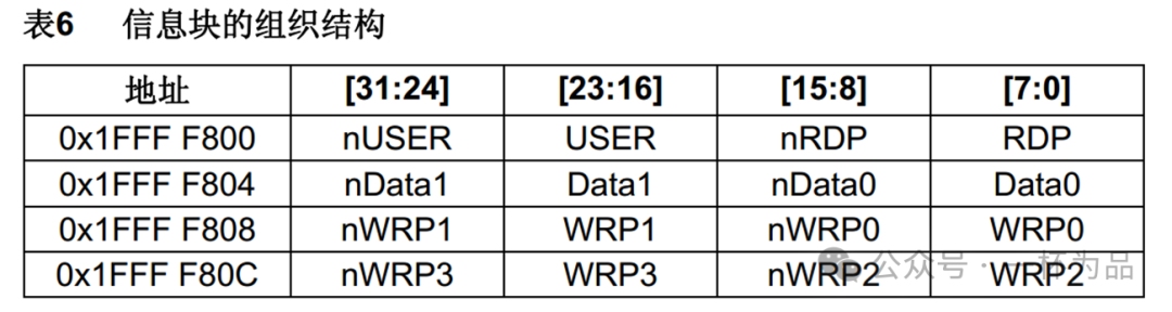
The address is the starting address for writing option bytes. The meanings of the names in the table are as follows:
- • RDP: Write RDPRT key to remove read protection, default is removed.
- • USER: Configure whether the hardware watchdog and entering sleep/standby mode will cause a reset.
- • Data0/1: User-defined usage.
- • WRP0/1/2/3: Configure write protection, each bit corresponds to protecting 4 storage pages (medium capacity). Small capacity products only need WRP0, while large capacity products use bit 7 of WRP3 to protect the remaining pages.
The prefix n requires that when writing to memory, the corresponding n-named location must also write the inverse code of the data for the write operation to be valid. If the chip detects that the two are not in an inverse relationship, it will not execute the corresponding function, which is a safety measure. The process of writing the inverse code is automatically completed by hardware and encapsulated in library functions.
Programming Option Bytes
- • Check the BSY bit of FLASH_SR to confirm that no other programming operations are in progress.
- • Unlock the OPTWRE bit of FLASH_CR.
- • The option bytes have a separate small lock, which can be unlocked by writing KEY1 and KEY2 to FLASH_OPTKEYR in sequence.
- • Set the OPTPG bit of FLASH_CR to 1.
- • Write the half-word to be programmed to the specified address.
- • Wait for the BSY bit to change to 0.
- • Read the written address and verify the data.
Erasing Option Bytes
- • Check the BSY bit of FLASH_SR to confirm that no other programming operations are in progress.
- • Unlock the OPTWRE bit of FLASH_CR.
- • Set the OPTER bit of FLASH_CR to 1.
- • Set the STRT bit of FLASH_CR to 1.
- • Wait for the BSY bit to change to 0.
- • Read the written address and verify the data.
Supplement
Writing a half-word to a FLASH address will initiate a programming operation, during which any read/write operations to FLASH will cause the CPU to pause until the FLASH programming is complete. If there are frequently executed interrupt functions that require strict timing, internal FLASH storage should be used with caution.
Device Electronic Signature
- • The electronic signature is stored in the system memory area of the flash memory module, containing chip identification information written at the factory, which cannot be changed. The electronic signature can be obtained by reading the memory at the specified address using pointers.
- • Flash capacity register:
- • Base address: 0x1FFFF7E0
- • Size: 16 bits
- • Unique product identification register:
- • Base address: 0x1FFFF7E8
- • Size: 96 bits
Function Details
FLASH_Unlock Function
Overview: Unlock FLASH.
Parameters: void
FLASH_Lock Function
Overview: Lock FLASH.
Parameters: void
FLASH_ErasePage Function
Overview: Erase FLASH page.
Parameters: Page starting address
Return Value: Execution status
FLASH_BUSY = 1 (busy)
FLASH_COMPLETE (execution complete)
FLASH_ERROR_PG (programming error)
FLASH_ERROR_WRP (write protection error)
FLASH_TIMEOUT (timeout)
FLASH_EraseAllPages Function
Overview: Full erase.
Parameters: void
Return Value: Execution status
FLASH_EraseOptionBytes Function
Overview: Erase option bytes.
Parameters: void
Return Value: Execution status
FLASH_Program(Half)Word Function
Overview: Write (half) word.
Parameter One: Write address
Parameter Two: (half) word data
Return Value: Execution status
FLASH_GetStatus Function
Overview: Get FLASH execution status.
Parameters: void
Return Value: Execution status
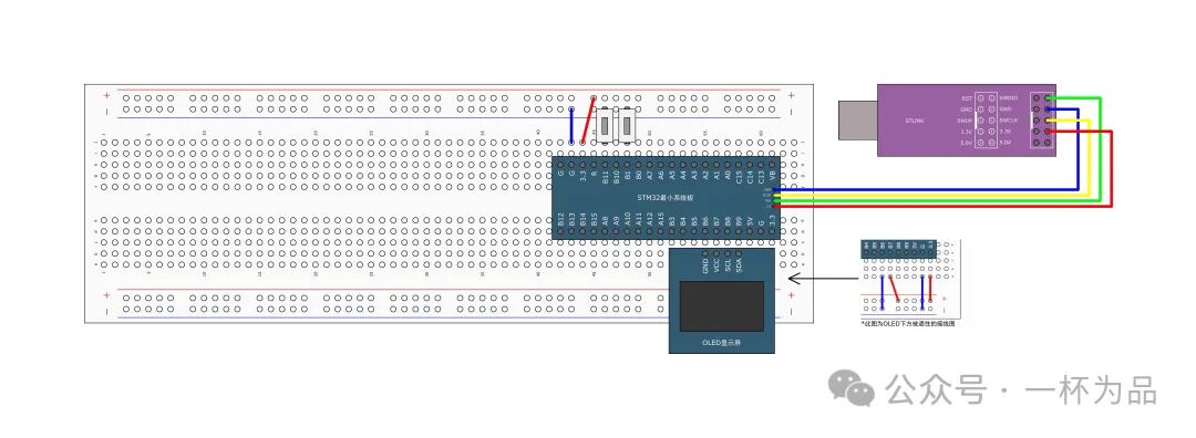
Experiment 36: Read and Write Internal FLASH
Functionality: Press Key1 to increment the array and immediately update it to FLASH; press Key2 to clear the array. After power-off, the array data is not lost.
Wiring Diagram
MyFLASH Driver
The driver file is located in the System folder.
MyFLASH.h
#ifndef __MYFLASH_H
#define __MYFLASH_H

uint32_t MyFLASH_ReadWord(uint32_t Address);
uint16_t MyFLASH_ReadHalfWord(uint32_t Address);
uint32_t MyFLASH_ReadByte(uint32_t Address);
void MyFLASH_EraseAllPages(void);
void MyFLASH_ErasePage(uint32_t PageAddress);
void MyFLASH_ProgramWord(uint32_t Address, uint32_t Data);
void MyFLASH_ProgramHalfWord(uint32_t Address, uint16_t Data);

#endif
MyFLASH.c
#include "stm32f10x.h"

// FLASH does not need initialization
// Read word
uint32_t MyFLASH_ReadWord(uint32_t Address)
{
    // Convert pointer to the corresponding data type pointer
    return *((__IO uint32_t *)(Address));
}

// Read half-word
uint16_t MyFLASH_ReadHalfWord(uint32_t Address)
{
    return *((__IO uint16_t *)(Address));
}

// Read byte
uint32_t MyFLASH_ReadByte(uint32_t Address)
{
    return *((__IO uint8_t *)(Address));
}

// Full erase
void MyFLASH_EraseAllPages(void)
{
    FLASH_Unlock();
    FLASH_EraseAllPages();
    FLASH_Lock();
}

// Page erase
void MyFLASH_ErasePage(uint32_t PageAddress)
{
    FLASH_Unlock();
    FLASH_ErasePage(PageAddress);
    FLASH_Lock();
}

// Write word
void MyFLASH_ProgramWord(uint32_t Address, uint32_t Data)
{
    FLASH_Unlock();
    FLASH_ProgramWord(Address, Data);
    FLASH_Lock();
}

// Write half-word
void MyFLASH_ProgramHalfWord(uint32_t Address, uint16_t Data)
{
    FLASH_Unlock();
    FLASH_ProgramHalfWord(Address, Data);
    FLASH_Lock();
}
Store Driver
Since directly reading and writing FLASH is inconvenient, inefficient, and prone to data loss, we define an array in SRAM as a surrogate for FLASH, directly operating on SRAM to read and write data. However, SRAM loses data on power-off, so we need FLASH to cooperate. Each time the SRAM is modified, the entire array is backed up to FLASH, and on power-up, the data from FLASH is initialized and loaded back into SRAM.
The driver file is located in the System folder.
Store.h
#ifndef __STORE_H
#define __STORE_H

extern uint16_t Store_Data[];

void Store_Init(void);
void Store_Save(void);
void Store_Clear(void);

#endif
Store.c
#include "stm32f10x.h"
#include "MyFLASH.h"

// Macro definitions for array storage location and array length
#define STORE_START_ADDRESS 0x0800FC00
#define STORE_COUNT 512

// A group of data corresponds to a page of FLASH of 1024 bytes
uint16_t Store_Data[STORE_COUNT];

void Store_Init(void)
{
    // Determine if FLASH has stored data based on custom 0xA5A5 flag
    if(MyFLASH_ReadHalfWord(STORE_START_ADDRESS) != 0xA5A5)
    {
        // If FLASH has not stored data, erase and write the custom flag
        MyFLASH_ErasePage(STORE_START_ADDRESS);
        MyFLASH_ProgramHalfWord(STORE_START_ADDRESS, 0xA5A5);
        // FLASH data defaults to 0xFFFF
        // Write 0 to all data except the flag to initialize the SRAM array to 0
        for(uint16_t i = 1; i < STORE_COUNT; i++)
        {
            // Each half-word occupies two bytes, so i*2
            MyFLASH_ProgramHalfWord(STORE_START_ADDRESS + i * 2, 0x0000);
        }
    }
    // On power-up, restore the backed-up data from FLASH (including the flag) to the SRAM array
    for(uint16_t i = 0; i < STORE_COUNT; i++)
    {
        Store_Data[i] = MyFLASH_ReadHalfWord(STORE_START_ADDRESS + i * 2);
    }
}

// Update the SRAM array (including the flag) to FLASH
void Store_Save(void)
{
        MyFLASH_ErasePage(STORE_START_ADDRESS);
        for(uint16_t i = 0; i < STORE_COUNT; i++)
        {
            MyFLASH_ProgramHalfWord(STORE_START_ADDRESS + i * 2, Store_Data[i]);
        }
}

// Clear data (except for the flag)
void Store_Clear(void)
{
    for(uint16_t i = 1; i < STORE_COUNT; i++)
    {
        Store_Data[i] = 0x0000;
    }
    // Each time the SRAM array is modified, update FLASH to ensure the array and FLASH are the same
    Store_Save();
}
Main Program
#include "stm32f10x.h"
#include "Delay.h"
#include "OLED.h"
#include "Store.h"
#include "Key.h"

uint8_t KeyNum;

int main(void)
{
    OLED_Init();
    Key_Init();
    Store_Init();

    // Display flag
    OLED_ShowString(1, 1, "Flag:");
    // Display data
    OLED_ShowString(1, 1, "Data:");

    while(1)
    {
        KeyNum = Key_GetNum();
        if(KeyNum == 1)
        {
            Store_Data[1]++;
            Store_Data[2] += 2;
            Store_Data[3] += 3;
            Store_Data[4] += 4;
            Store_Save();
        }
        if(KeyNum == 2)
        {
            Store_Clear();
        }
        OLED_ShowHexNum(1, 6, Store_Data[0], 4);
        OLED_ShowHexNum(3, 1, Store_Data[1], 4);
        OLED_ShowHexNum(3, 6, Store_Data[2], 4);
        OLED_ShowHexNum(4, 1, Store_Data[3], 4);
        OLED_ShowHexNum(4, 6, Store_Data[4], 4);
    }
}
Program Space Modification
To avoid conflicts between program space and array storage space, you can manually adjust the program allocation space in Keil5.
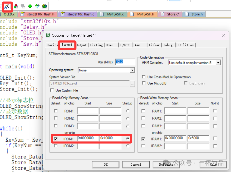
The on-chip ROM starting address (program starting address) is 0x8000000 (the highest bit 0 is omitted), and the size is 0x10000, with the default allocation of all 64K FLASH for program code. You can reduce the size a bit to reserve the tail space of FLASH. If the size is too small, a compilation error will occur to prompt us to adjust. The right side IRAM1 shows the starting address and size of on-chip RAM.
By compiling the entire program, you can obtain the program size from the compilation output:
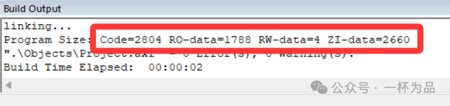
The sum of the first three numbers is the size of FLASH occupied, and the sum of the last two numbers is the size of SRAM occupied.
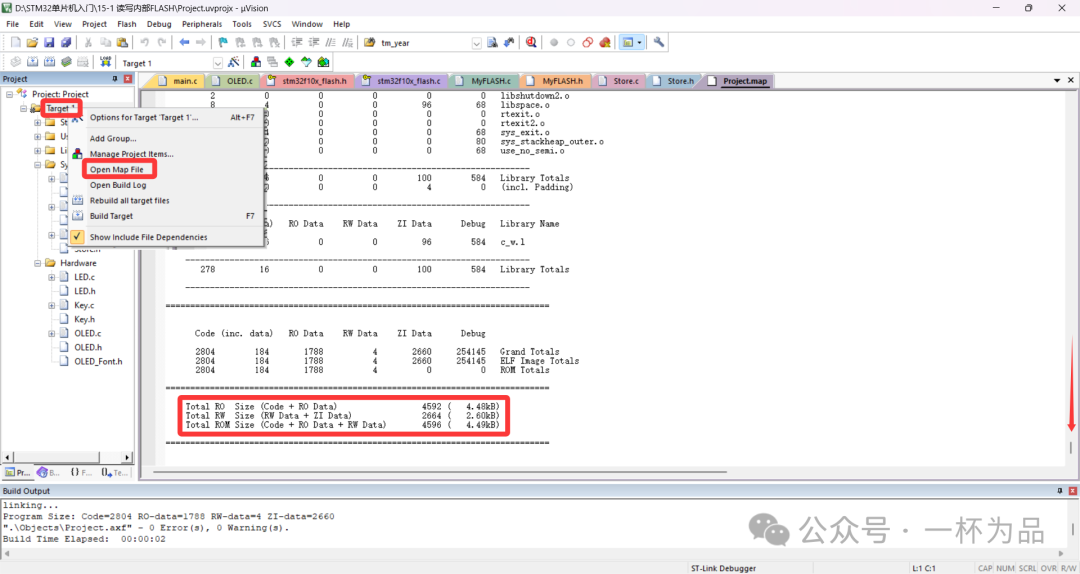
You can also check in the Target’s map file:
Experiment 37: Read Chip ID
The wiring only requires the OLED module.
This experiment mainly demonstrates how to read register data using pointers.
#include "stm32f10x.h"
#include "Delay.h"
#include "OLED.h"

int main(void)
{
    OLED_Init();

    // Display FLASH capacity
    OLED_ShowString(1, 1, "F_SIZE:");
    OLED_ShowHexNum(1, 8, *((__IO uint16_t*)(0x1FFFF7E0)), 4);
    // Display chip ID
    OLED_ShowString(2, 1, "U_ID:");
    // Chip ID is stored in multiple memory locations, read sequentially by address offset
    // The following shows both 16-bit and 32-bit reading methods
    OLED_ShowHexNum(2, 6, *((__IO uint16_t*)(0x1FFFF7E8)), 4);
    OLED_ShowHexNum(2, 11, *((__IO uint16_t*)(0x1FFFF7E8 + 0x02)), 4);
    OLED_ShowHexNum(3, 1, *((__IO uint32_t*)(0x1FFFF7E8 + 0x04)), 8);
    OLED_ShowHexNum(4, 1, *((__IO uint32_t*)(0x1FFFF7E8 + 0x08)), 8);
    while(1)
    {
    }
}