
Source
Title:SIMD in the GPU World Address: https://www.rastergrid.com/blog/gpu-tech/2022/02/simd-in-the-gpu-world/Abstract: Today, SIMT has almost become synonymous with GPUs, while the SIMT defined by Flynn originally was just a form of SIMD. The technology itself has only similarities and differences, with no inherent superiority or inferiority; the key is to use the appropriate technology in the right context. This article will trace the role of SIMD in the evolution of GPU architecture. Without the increasingly flexible application of the SIMD paradigm in modern processors, the current high computational throughput might not be achievable. GPUs have also gained most of their performance, chip area, and efficiency advantages from this instruction dispatch scheme, which is no coincidence. In this article, we will explore how GPUs leverage SIMD through several examples and the implications of these examples on programming models. Before continuing the discussion, note that we will not discuss processor hardware design; thus, various components within processor cores, superscalar processor architectures, instruction issue ports, instruction-level parallelism, register files, bank conflicts, etc., will not be covered in this article. We will focus on the various uses of the SIMD paradigm, which will directly impact how developers write efficient code for such processors, alongside a slight mention of other topics. However, this does not mean that hardware details and other nuances between specific target architectures do not significantly affect how to write code for optimal performance; it simply means these topics are outside the scope of this article.What is SIMD?This term comes from Flynn’s classification based on computing architectures. SIMD stands for Single Instruction Multiple Data, in contrast to SISD, which refers to the Single Instruction Single Data of the traditional von Neumann architecture. SIMD is a parallel processing technology that executes the same instruction on multiple data elements simultaneously, achieving data-level parallelism.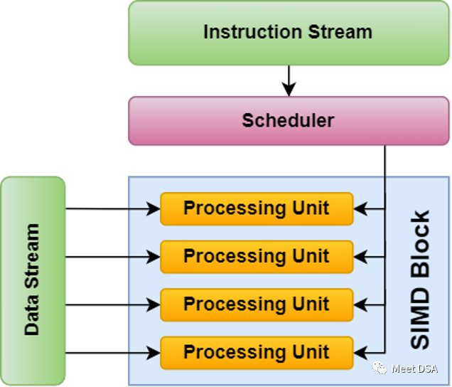 Example of a 4-lane SIMD block From different perspectives, SIMD supports the simultaneous use of a single instruction scheduler across multiple processing units. Compared to traditional scalar processing cores that use a one-to-one mapping between instruction schedulers and processing units, SIMD allows processor designers to save significant chip area, thereby achieving higher computational throughput with the same number of transistors. The SIMD model is not unique to large-scale parallel processors like GPUs; in fact, CPUs have a long history of using SIMD instruction sets. In addition to the traditional scalar operations provided by CPUs, SIMD instruction sets like MMX, SSE, NEON, and AVX can be utilized. Although our focus is on GPUs, we will also see several examples related to CPUs.Vector SIMD In the past, 3D graphics applications were primarily vector operations, and to some extent, they still are:
-
Rendering 3D scenes requires linear transformations of geometric properties (position, normal, and texture coordinates), involving vector-matrix multiplication, which consists of multiple vector-to-vector operations (dot products) typically performed on 4-component vectors.
-
Determining the color of a single vertex and/or pixel often involves complex lighting calculations, which usually include 3 or 4-component vector operations, where vectors represent colors (RGB or RGBA format) or directions (such as surface normals, incident light directions, reflection directions, etc.).
Therefore, it is not surprising that GPUs have been using SIMD units to implement vector instructions since their early days. The earliest programmable shaders used assembly-like shading languages that provided instructions for operating on 4-component vectors, which is also not coincidental. In this model, the atomic unit of data is a 4-component vector containing floating-point operands. Assuming the use of standard IEEE 754 32-bit floating-point values, we can obtain a vector register with a total width of 128 bits. This form of SIMD that operates on multi-component registers is often referred to as Packed-SIMD or SWAR (SIMD within a register). The following two types of instructions (or instruction series) are particularly noteworthy. The first type is MAD (multiply-add) or MAC (multiply-accumulate), which can be used as a single instruction on almost all GPUs, as graphics and multimedia applications are all about scale and bias operations. This means that on traditional 4-component vector-based GPUs, a single instruction is required to compute 4 floating-point multiplications and 4 additions, and floating-point MAD/MAC is still commonly used as a unit of measurement for GPU instruction throughput. The second type includes various dot product instructions (such as DP4 or DP3) used to compute the scalar (or dot) product of two vectors. These instructions themselves contain MAD/MAC operations to a greater or lesser extent, making execution on vector SIMD processors relatively straightforward. Since most transformations and lighting calculations are directly or indirectly comprised of dot products, vector SIMD processors benefit significantly from single instructions in terms of throughput and latency.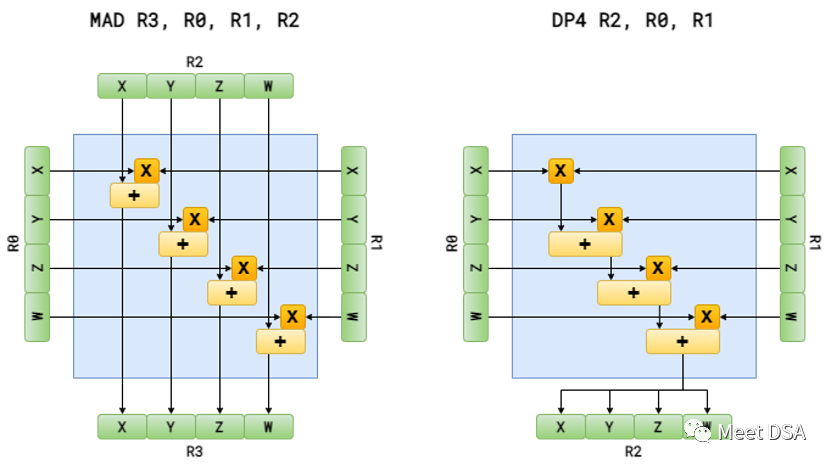 Possible implementation example of 4-component Multiply-Add (MAD, left) and Dot Product (DP4, right) pipelines Since processing time is primarily dominated by multiplication operations, the latency for completing these two operations is roughly the same. It is also worth noting that the scalar result of the DP4 instruction is typically copied between channels in the destination vector register by default (unless specified otherwise, which we will introduce next). CPU SIMD instruction sets also utilize packed-SIMD technology. For example, on x86, the XMM registers can be viewed as packed vectors containing multiple elements, allowing the SSE instruction set to perform single-instruction operations on multiple data elements. When discussing vector SIMD processors, two key technologies that have gained popularity should be noted:
- Operand Reorganization (component swizzling): The ability to redirect individual operands of the source operation to a single processing unit, similarly redirecting a single output operand to the target operand
- Operand Masking (component masking): The ability to discard a single output operand (or similarly disable a single processing unit)
More complex variants of the same operation can be expressed by reducing the number of components to be processed, copying inputs or outputs between components, etc. Operation implementations usually also support special constant reorganization, where corresponding components of the operation are replaced by some commonly used constant values, such as 0.0, 1.0, 2.0, and 0.5 (and possibly more). Allowing all (or at least most) instructions to perform custom reorganization and masking can significantly reduce the number of instructions required for established applications, as this reduces the demand for most movement instructions.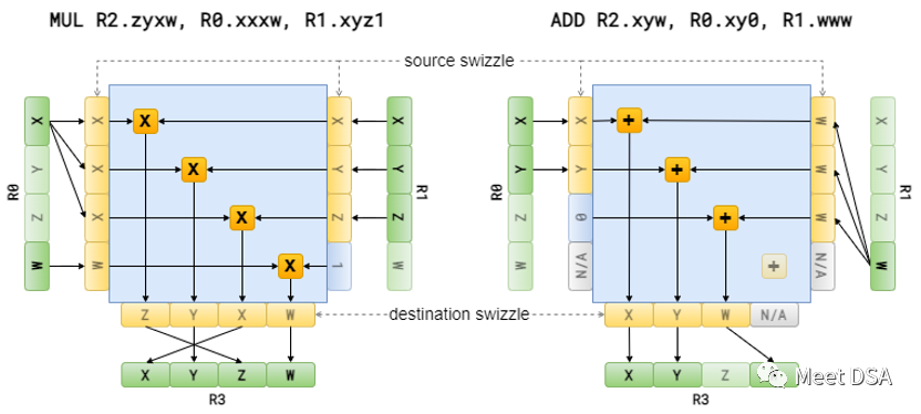 Illustration of Reorganization (left) and Masking (right) in Vector Instructions Note that in the example on the right, the third component (Z) of the output is masked, but in reality, the fourth channel of SIMD is unused. The latter is arbitrary; in fact, different SIMD instruction sets represent masking in different ways (which we will see later). Although traditional vector-based GPUs are no longer popular, packed-SIMD technology is still applied in other ways, which we will see later.Vector to Scalar As GPU applications evolve, an increasing number of scalar operations appear in shaders, making it increasingly difficult for traditional vector-based GPUs to achieve theoretical computational throughput. Since these processors were designed with vectors in mind, executing scalar operations typically means executing a vector instruction where all components except one are masked. While it is sometimes possible to combine multiple scalar operations into a single vector instruction, for example, four separate scalar additions can be simply merged into a single vector addition, utilizing all processing units, it is generally challenging to find enough independent scalar operations of the same type. Nevertheless, when facing vector-based GPUs or other packed-SIMD instruction sets, it is often strongly recommended to use vectorized computations, as application developers tend to perform better in this regard compared to optimized compilers. Therefore, some GPUs have transitioned from traditional vector-based architectures to VLIW architectures. VLIW stands for Very Long Instruction Word; processors using this type of instruction set can utilize complex instructions composed of multiple parallel execution operations. Some VLIW-based GPUs use a 3+1 structure, where one instruction encodes an operation for the first three components of the vector register and encodes a different operation for the fourth component. This is because RGBA values usually require different operations for the RGB color channels and the alpha channel. For many computations, 3-component vector operations suffice (only color, directional vector, or affine transformation operations), leaving the fourth processing unit free for executing other operations, such as a completely independent scalar operation.
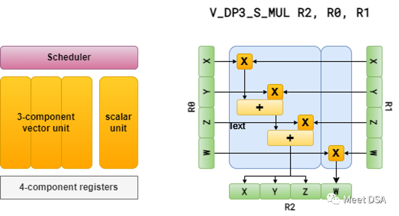 Illustration of Hypothetical 3+1 VLIW Processing Core (left) and Example Instruction Combining 3-component Vector and Scalar Operations (right) Beyond operations (such as trigonometric and logarithmic operations) and other non-trigonometric operations typically used only for scalar operations (division, square root, etc.), are generally performed on the fourth processing unit (referred to as the Transcendental Unit), aligning with processor design and better accommodating expected applications while saving valuable chip area. Over time, VLIW-based GPUs have become increasingly complex, featuring various widths and specifying multiple operations within a single instruction in a more flexible manner. In their most complex versions, VLIW instruction sets can allow any scheduling operation for each component individually. Therefore, compared to traditional vector-based GPUs, VLIW-based GPUs can allow almost all operations to be merged into a single VLIW instruction, covering the entire processing block width, as each instruction can vary based on components (or tuples), not just data. However, these operations typically require independence, meaning that within a single instruction, no operation source can depend on the result of another instruction. Thus, even if application developers and compilers make maximum optimization efforts, due to data dependencies, multiple processing units may still be idle during shader calls. Additionally, unless a specific instruction set supports using different registers as source or target operands through different operations within a single VLIW instruction, additional movement operations may be required to achieve operand address constraints, similar to traditional vector-based GPUs. However, one of the advantages of such architectures is the ability to operate in a hybrid mode, meaning both vector and scalar operations can be represented within a single instruction. Therefore, even inter-component vector operations, such as dot products and cross products, can be accomplished through a single instruction (though the actual time to complete the instruction may vary depending on the operations used). Moreover, the heterogeneous instruction set of such processors means that the instruction decoder and scheduler are likely equally complex, thus limiting the chip area advantage of using a single instruction scheduler across multiple processing units. One way to reduce this complexity is to use a simple scalar instruction set instead, such as AMD’s GCN instruction set architecture, which may be the most well-known GPU ISA in the developer community to date. Of course, there are trade-offs, as in a fully scalar instruction set, even basic dot product operations require multiple MAD/MAC instructions (though we again overlook some important details, such as the actual time taken by each instruction). In this paradigm shift, it has become increasingly important for application developers to use scalar operations as much as possible in shaders, performing vector operations only within the natural granularity of the computation. But does all of this mean that we have completed the development of SIMD? Certainly not; in fact, we have only just begun…SIMT Vector processing is just one way to take advantage of the SIMD paradigm. Another common method of utilizing SIMD instructions is through Array Processing (as opposed to vector processing), typically performed on CPUs, as shown in the example below: As can be seen from the above, although the individual work to be performed on array elements is essentially scalar, SIMD instructions can be used to process multiple array elements in parallel. This subtype of SIMD pattern is commonly referred to as SIMT, or Single Instruction Multiple Threads. To some extent, this description is slightly inaccurate, as the “threads” we are discussing here are not the independently schedulable execution threads we are familiar with, but rather the threads from NVIDIA’s CUDA API, which are independent lanes within a wave. But let’s not jump to conclusions too early. This is, in fact, the other side of the same coin; if we really think about it, we could also refer to the above example as vectorization. However, when this vectorization is not explicit but rather a product of the programming model, the distinction between array processing and vector processing becomes evident. So far, we have only discussed leveraging internal parallelism within a single shader call, as many shaders operate on vectors of different widths, and sometimes even scalar operations are mutually independent. However, the massive parallelism of GPU applications actually comes from the need to execute the same shader code across a large number of data elements (vertices, primitives, fragments, etc.). Therefore, ignoring control flow for the moment, early programmable GPUs did not possess this capability, and increasing the width of SIMD units proportionally could easily process multiple shader calls in parallel. Of course, the width of SIMD units is limited in practical applications and technology, but theoretically, it can reach the width of the entire processor. This allows for more reuse of a single instruction scheduler across multiple processing units compared to vector-based or VLIW-based processors.
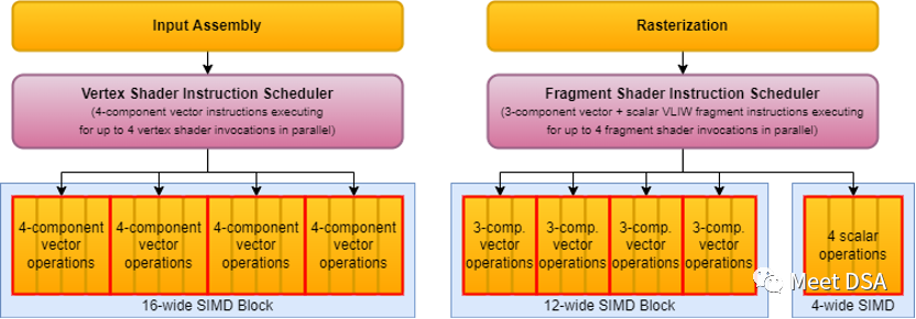 Illustration: Assuming the GPU contains a vector-based vertex processor and a 3+1 VLIW fragment processor Returning to GPUs using scalar instruction sets, it is not difficult to find that the scalar nature of the instructions themselves does not prevent us from utilizing SIMD technology, just like their vector or VLIW counterparts, the instruction stream can be issued simultaneously across multiple shader calls or roughly executed in a lockstep manner. In practice, current GPUs typically consist of multiple groups of SIMD processing blocks, which are hierarchically aggregated into clusters that share various types of caches and auxiliary hardware areas to perform fixed-function operations in the graphics pipeline. In this model, scheduling one or more shader calls in the processing units simultaneously constitutes a subgroup, often also referred to as a wave, wavefront, or warp, with individual shader calls referred to as lanes or threads of the wave. Taking AMD’s GCN architecture as an example, even though these instructions are scalar instructions from the perspective of a single shader call, they are actually referred to as vector instructions, as they are executed across the entire wave through wide vector operations, where each component belongs to a specific shader call. Therefore, the scalar nature of the instruction set should not be confused with the scalar units available on GCN GPUs (or recent NVIDIA GPUs), which are actually more akin to SISD execution units shared across the entire wave.SIMD Control Flow Over time, GPUs have been able to support increasingly complex shader control flows. However, if SIMD units can handle multiple shader calls (or threads), the implementation of control flow becomes less intuitive. At this point, another SIMD mode comes into play, referred to in Flynn’s classification as Associative Processors. This technique somewhat extends the concept we mentioned when discussing vector-based GPUs earlier, where individual components can be masked within vector operations. For SIMD units processing multiple shader calls in parallel, there is no reason we cannot adopt the same approach. Early GPU control flow did not have true branch support within processors; specifically, there were no jump instructions or anything similar available. Therefore, compilers would undertake any type of loop, and shader developers had to be mindful of the instruction limitations of the target GPU; at this point, instructions were not flowing out of memory but were stored in a limited-size on-chip buffer. However, support for conditions appeared early on in the form of predicate/conditional instructions. In a simple implementation, in the case of an if-else block, the GPU would execute both branches, and a conditional instruction (such as some form of CMOV) would select the corresponding branch’s result based on the condition’s value. This allows for the continued use of SIMD technology to execute multiple shader calls in parallel while allowing individual calls to actually execute different branches in control flow.
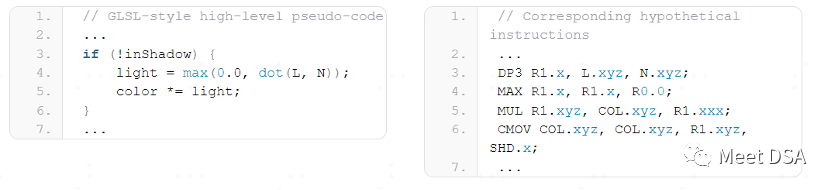 Clearly, this incurs a hefty cost, as all branches in the shader must be executed for any shader call. This is why it was previously recommended to avoid conditional instructions in shaders whenever possible, as the lack of true branching functionality would far exceed the actual GPU. Nevertheless, even during these periods, when the computations in actual branches were quite limited, the cost of control flow was still acceptable, as illustrated in the above example. One downside of using the above method is that we not only pay the performance cost of two branches but also their power cost, as all shader calls in the SIMD unit execute both sets of calculations, even if each branch ultimately only uses the result of one of them. Therefore, in practice, GPUs support evaluating almost every instruction through some special registers, similar to mask registers used in CPU instruction sets like AVX-512. Thus, even early assembly-like shading languages employed this method to at least save power costs for specific branches not used in shader calls.
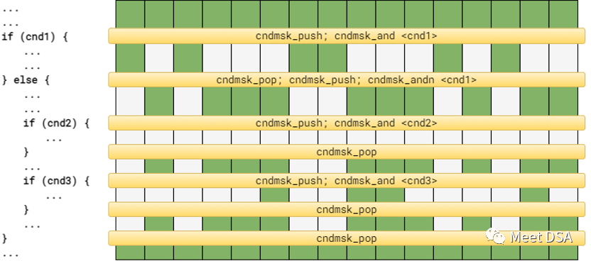 Illustration: During the execution of 16 shader calls, assuming the condition (predicate) mask of active lanes for a 16-wide SIMT GPU, different branches take different paths. The green lanes are active, while the gray lanes are masked accordingly. Note that this is an implementation using a stack to handle nested conditions. In a non-stack implementation, flattening nested conditions can typically be achieved through other methods. More commonly, since the nesting depth of shaders is usually known, a fixed number of backup registers can be used as a stack. In the absence of branch instruction support, even if there are no shader calls in the wave, this branch will still be used and cannot be skipped, as shown by the branch of cnd2 above. Later, updated GPUs introduced actual branch instructions (similar to jumps or structured ones), which work similarly to their SISD versions. However, it is important to remember that GPUs schedule and execute shader calls in a lockstep manner for the entire wave, so branch instructions can only skip code if all shader calls in the wave take the same path. Unlike the situation we discussed regarding branch divergence in waves, similar to previous generations, GPUs execute both branches of if-else blocks simultaneously, or worse, in the case of loops, meaning that each shader call in the wave incurs the time of the longest call. While the control flow cost is low for current GPUs, there is a tendency to favor dynamic uniform control flows (not divergent control flows), avoiding the execution cost of mutually exclusive branch instructions for multiple shader calls.
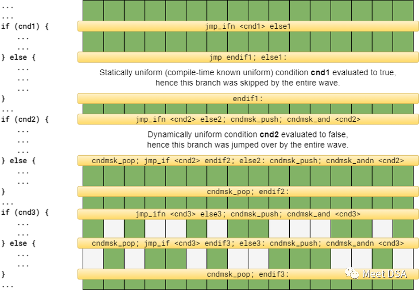 Illustration: During the execution of 16 shader calls, assuming support for 16-wide active lanes in the SIMT GPU. The green lanes are active, while the gray lanes are masked accordingly. Note the following points:
- cnd1 is a compile-time known uniform expression, meaning that from the shader code, it can be determined that the conditions will not change across different lanes in a wave, so only a branch instruction is needed.
- cnd2 is a dynamically uniform expression, meaning that all lanes in the wave will evaluate to the same value, allowing the wave to skip unexecuted branches. However, since dynamic uniformity is unknown at compile time, the compiler still needs to add conditional mask code.
- cnd3 is a divergent expression, meaning the wave will execute both branches through appropriate predicates.
-
If the shading language syntax allows for such expressions, it can avoid generating branch code for known divergent branches or predicate code for known dynamic uniform branches.
Cross-lane Operations Similar to component masking extending to instruction predicates in the SIMT model, component reorganization has a corresponding method, known as cross-lane operations. When using vector components as instruction operands on vector-based GPUs, rather than reorganizing the components of the vector, data reorganization occurs among shader calls within a wave. This has become one of the hottest shading language features in recent years, as it allows for higher-performance data sharing between shader calls within a subset, compared to the slower data exchanges performed across a broader range (work group) in shared memory. Cross-lane operations enable shader calls to directly reference data in registers of other shader calls within the wave. Considering that all shader calls executed on a specific SIMD unit’s registers reside in the same register file, achieving this seems relatively straightforward.More Content Processors typically adopt another approach to enhance instruction-level parallelism without actually increasing the width of the underlying SIMD blocks. In this scheme, the instruction scheduler issues each instruction multiple times but targets different sets of shader calls, usually referred to as Temporal SIMT, or when using wide SIMD blocks, referred to as Spatio-Temporal SIMT, as instruction issuance occurs in both the spatial domain (across various lanes of the SIMD block) and the temporal domain. Roughly speaking, this is similar to using the REP prefix for string operations on x86 CPUs, though this is not an accurate analogy. In practice, temporal SIMT on GPUs is usually stricter than this, as the number of instruction re-issues is generally hard-coded. For example, AMD’s GCN architecture issues shader call instructions for a complete 64-wide wave to a 16-wide SIMD module over 4 cycles (16 lanes per cycle). This instruction execution technique can hide delays in instruction decoding and/or execution, thus providing greater instruction-level parallelism. However, note that this technique should not be confused with the commonly used simultaneous multithreading (SMT) on GPUs, which refers to scheduling instructions for other waves while one wave is waiting for long-latency operations (such as memory reads). Temporal SIMT can also be implemented in a basic form, meaning there are no actual wide execution units. In this case, each shader call in the wave is issued in separate cycles and may even skip issuing instructions for inactive shader calls due to predicate execution. This approach can eliminate the costs of divergent shader calls but only to a certain extent, as it also limits the opportunity to hide operational execution delays, thus constraining effective instruction-level parallelism and increasing the overall time to complete wave execution due to the removal of a dimension of parallelism. Another technique is to share a single instruction scheduler among multiple SIMD modules. While this may not be obvious, issuing instructions to multiple SIMD blocks differs from issuing them to a single wider SIMD block. For instance, separate SIMD modules have distinct register files, so even if fed data by the same instruction scheduler, simple cross-lane operations cannot be performed between shader calls running on separate SIMD modules. Combining temporal SIMT with a single instruction scheduler across multiple SIMD modules allows a single scheduler to handle more concurrently executing instructions. However, this may sometimes mean that the issuance granularity might exceed the size of a single wave. For example, in AMD’s GCN architecture, this is not the case, as a single instruction for a 64-wide wave takes 4 cycles to initiate on a single 16-wide SIMD block. Although each scheduler has four SIMD blocks, the scheduler can actually issue one instruction from a single wave in each cycle, thus being able to send a new instruction to all four SIMD blocks within those 4 cycles until it must return to the first SIMD block.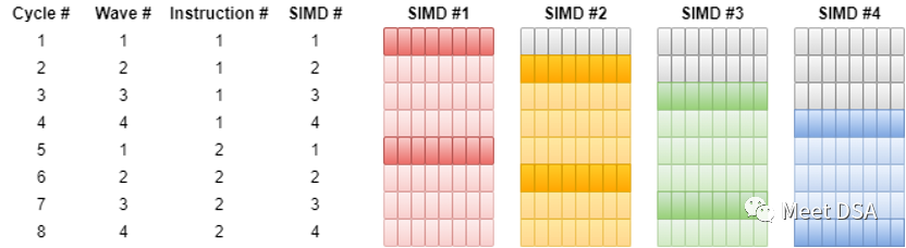 Illustration: How a Spatio-Temporal SIMT GPU uses a single scheduler to issue instructions from a 32-wide wave to four 8-wide SIMD execution units The dark blocks represent the first instance of instruction issuance (covering the first 8 shader calls in the wave), while the light blocks represent subsequent groups of shader calls in the same wave reissuing the same instruction. Although some of the techniques introduced for utilizing SIMD patterns may seem mutually exclusive, all of these techniques can be combined. For example, there is no reason why vector-based or VLIW-based GPUs cannot utilize the SIMT model; in fact, they do leverage the SIMT model, as the 4-wide SIMD is insufficient to achieve the scale of computational throughput we have seen on GPUs over the past decades. Another example of multi-paradigm applications of SIMD processing is that for some SIMT-based GPUs, supporting multiple operation precisions (such as 16-bit and 32-bit floating-point operations) may mean that even GPUs using scalar instruction sets could perform lower-precision operations according to packed-SIMD paradigms or use wider vector widths for lower-precision operations, as register widths are typically fixed by architecture.
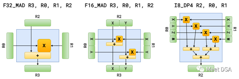 Illustration: Mixing scalar and vector (packed-SIMD) pipelines on a 32-bit register GPU Conclusion As we have seen, GPUs can leverage the advantages of the SIMD paradigm in many beneficial ways. However, all of these techniques will affect how code is written to varying degrees to maximize performance. It is crucial for developers to be familiar with these techniques. Fortunately, various types of technical implementations have a high degree of commonality, so there will not be much missed. Nevertheless, there will always be some additional performance considerations for specific hardware architectures. It is also worth noting that to some extent, the instruction set and the way the actual processor schedules the execution of individual operations are orthogonal; not to mention the execution itself. We have illustrated how hardware executes computations in SIMD in a very simplified manner. The deep instruction pipelines of modern superscalar processors are far more complex than this. Furthermore, the way instruction sets map platform-independent shader code to instruction sets is often hidden within the compiler infrastructure provided by hardware vendors. Therefore, it can sometimes lead to incorrect conclusions about how to encode for specific target hardware based on some limited high-level information that is architecture-related. Considering the various graphics and compute APIs providing shader programming models, it appears that at least the SIMT execution model is universal across all GPU architectures on the market today, while other design choices (such as using vector-based, VLIW, or scalar instruction sets—or combinations of these instruction sets) exhibit significant differences in various implementations. In fact, it is not uncommon for current GPUs to switch between various issuance models (e.g., vector versus scalar, or different wave widths seen in some of the latest architectures). Perhaps it is this flexibility and granularity of the switchable issuance models that define each unique architecture. If GPU architectures continue to evolve in this multi-paradigm direction, it could be good news for application developers, as this may lead to better performance and efficiency through more algorithm implementations.© THE END This translation is for reference only. Please contact this public account for authorization to reproduce.