Banner | Promotion
Micro-LED (Micro-LED) display is an innovative technology with broad application prospects, occupying an important position in display technology. Micro-LED has advantages such as high brightness, low power consumption, long lifespan, short response time, and high stability. It can be applied to small displays like Virtual Reality (VR), Augmented Reality (AR), and mobile phones, as well as medium to large displays like home TVs and conference walls, showing good development potential in the display field. Its excellent performance can meet the personalized needs of high-end displays, such as: 5G ultra-high-definition displays, AR glasses, medical displays, and automotive displays. In recent years, numerous research institutions and enterprises worldwide have conducted in-depth research on Micro-LED display technology, successfully developing various high-performance Micro-LED display prototypes or products using different process technologies.
Recently, the research team led by Associate Professor Zheng Hua from Dongguan University of Technology collaborated with the team of Researcher Ning Honglong from South China University of Technology to publish a review article titled “Research Progress on Micro-LED Display and Its Driving Technology” in the journal Liquid Crystal and Display (ESCI, Scopus indexed, Chinese core journal) in the 11th issue of 2022.
The article reviews the development history and research achievements of Micro-LED display technology since 2000, analyzes array preparation and flip-chip integration technology, and focuses on the research of Micro-LED display driving technology. Micro-LED display driving technology is divided into passive driving (Passive Matrix, PM) and active driving (Active Matrix, AM) methods, mainly introducing the circuit principles of passive driving, as well as the complementary metal-oxide-semiconductor (CMOS) driving technology, thin-film transistor (TFT) driving technology, and active pixel driving circuits for active driving.
1. Micro-LED Display Technology 1.1 Development History
In 2000, Jiang Hongxing and others from Kansas State University in the USA prepared Micro-LED based on group III nitride and reported in 2001 the successful fabrication of a 10×10 blue Micro-LED array using passive driving, laying a theoretical foundation for the development of Micro-LED displays. Since the concept of Micro-LED was first proposed, it has become one of the key technological focuses in international competition in recent years. Currently, China is also heavily investing in research on Micro-LED technology in its “14th Five-Year Plan”.
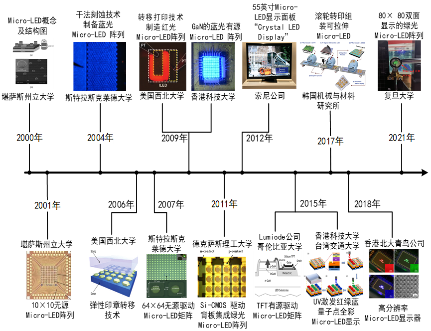
Figure 1: Development History of Micro-LED
Source: Liquid Crystal and Display, 2022, 37(11): 1395-1410. Fig.1
1.2 Micro-LED Array Process and Integration Technology
RGB three primary colors are prepared based on different materials, such as InGaN/GaN-based materials for green/blue Micro-LED arrays and AlInGaP/GaAs-based materials for red Micro-LED arrays. Generally, the epitaxial layers are grown on substrates like sapphire, gallium arsenide, and silicon to prepare Micro-LED arrays. Taking the preparation of GaN Micro-LED arrays on sapphire substrates as an example, firstly, metal-organic chemical vapor deposition (MOCVD) technology is used to grow the epitaxial layers on the sapphire substrate, including the n-GaN layer, MQW layer, and p-GaN layer; subsequently, the p-GaN layer and MQW layer are etched to isolate the pixels, forming a mesa structure; then, a current spreading layer is deposited on the p-GaN layer; and a p-electrode layer is deposited on the current spreading layer, while an n-electrode layer is deposited on the n-GaN layer, followed by a passivation layer; the final step is to construct n-type and p-type contact pads. The constructed contact pads facilitate subsequent chip integration, connecting the n-electrodes of the Micro-LED pixels together and connecting the p-electrodes to the output terminals of the driving circuit on the AM backplane, as shown in the specific process flow in Figure 2.
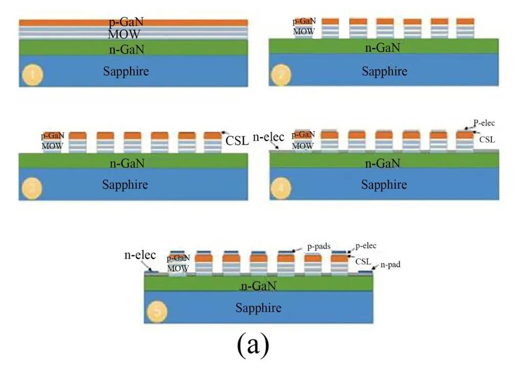
Figure 2: Process Flow Diagram for Micro-LED Array Fabrication
Source: SID Symposium Digest of Technical Papers, 2018, 49(S1): 272-275.
After peeling the Micro-LED from the original substrate, transfer technology is needed to bond the Micro-LED array to the driving substrate. The two commonly used bonding methods include traditional wire bonding and improved flip-chip bonding, as shown in Figure 3. Large pixel displays and passive matrix driving circuits typically use wire bonding, as shown in Figure 3(a), where the horizontal electrodes of the Micro-LED devices are connected to the n and p contact pads with gold wires for contact. This method is easy to implement, low cost, but has poor heat dissipation capabilities, is size-limited, and is not suitable for high-resolution displays. In active driving displays, the n-electrodes of the Micro-LED array are connected to the ground, while the p-electrodes are independently connected to the driving circuit, using flip-chip bonding technology, where each Micro-LED pixel is bonded to the corresponding CMOS driving circuit, which can store data and drive each individual Micro-LED pixel, as shown in Figure 3(b).
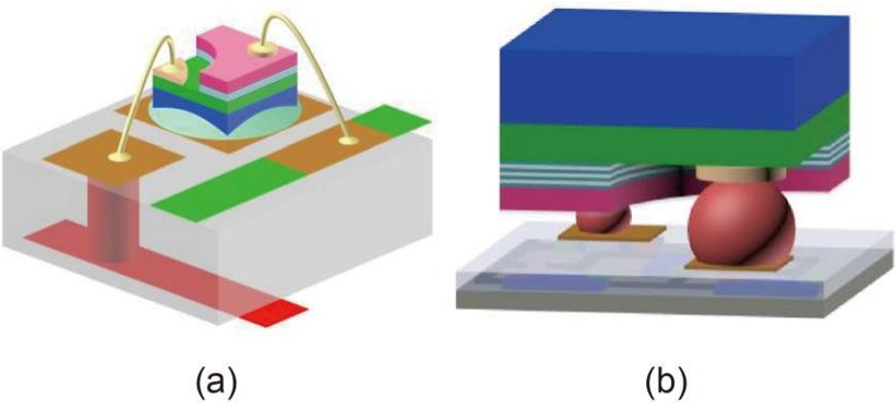
Figure 3: Pixel Bonding Methods (a) Wire Bonding; (b) Flip-Chip Bonding.
Source: SID Symposium Digest of Technical Papers, 2018, 49(S1): 272-275.
2. Micro-LED Driving Technology
Micro-LED display technology has two driving methods: passive driving (PM) and active driving (AM). The structure of the Micro-LED pixel unit driving circuit varies depending on the driving method. Since passive driving uses a scanning method, only one row of pixels is lit at any given moment, resulting in a very low duty cycle, making it unsuitable for large-size displays. In contrast, the active driving method allows independent control of each pixel, which is the main focus of current research.
2.1 Passive Driving Technology
The passive driving method connects the anodes (P-electrode) of each column of pixels to column data, while the cathodes (N-electrode) of each row of pixels are connected to row scanning lines. When a specific row and column have a current signal passing through, the pixel unit at the intersection of the row and column will be lit. By applying different voltages to each pixel row by row, each pixel can achieve different brightness displays, dynamically displaying images in a matrix manner. The use of Micro-LED passive driving technology can lead to issues such as excessive current density, crosstalk between wires, and impedance deviations due to different wiring lengths on the matrix, which limits the resolution, brightness, reliability, and picture quality of Micro-LED displays. The equivalent circuit diagram of Micro-LED passive driving is shown in Figure 4.
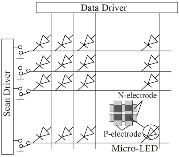
Figure 4: Equivalent Circuit Diagram of Passive Driving
Source: Liquid Crystal and Display, 2022, 37(11): 1395-1410. Fig.6
In 2014, Liu Zhaojun and others prepared a 0.19-inch 1700 PPI blue passive matrix Micro-LED display, with a display area of 3.8×2.9 mm², consisting of 256×192 pixels. This display uses passive driving technology, does not require the preparation of CMOS/TFT driving, but requires etching the GaN chip to the sapphire substrate, allowing the n and p electrodes between the LED pixel units to remain independent, forming individual Micro-LED pixels, as shown in the fabrication process in Figure 5.
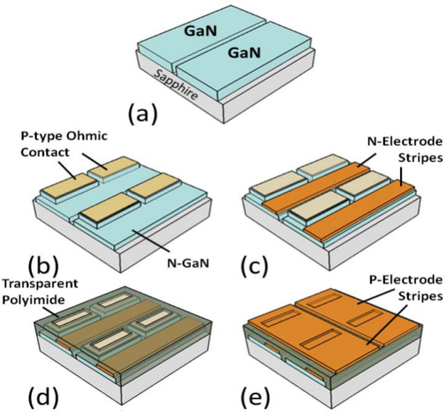
Figure 5: Passive Matrix Fabrication Process Diagram. (a) Forming Isolation Trenches; (b) Pixel Patterning and Deposition of p-type Ohmic Contacts; (c) Deposition of Striped n-type Electrodes; (d) Coating Transparent Polyimide; (e) Deposition of Striped P-type Electrodes
Source: 2014 IEEE Compound Semiconductor Integrated Circuit Symposium (CSICS). La Jolla, CA, USA: IEEE, 2014: 1-4.
2.2 Active Driving Technology
In active driving circuits, each Micro-LED pixel has its own independent driving circuit, and the dual-transistor single-capacitor 2T1C circuit is the most basic active matrix driving circuit. A single 2T1C pixel circuit uses 2 TFT transistors and 1 capacitor, where T1 is a switching transistor used to control the opening or closing of the pixel circuit, and T2 is the driving transistor, connected to the voltage source VDD, providing stable driving current to the Micro-LED within a frame, relying on the storage capacitor Cs to store the Vdata data signal. The active driving method overcomes the crosstalk issues present when pixels are scanned, allowing pixel units to have longer lighting times, resulting in higher display brightness for Micro-LED displays. Figure 6(a) shows the 2T1C active matrix pixel circuit, and the configuration of the driving circuit panel on the active panel is shown in Figure 6(b).
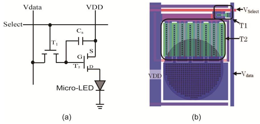
Figure 6: (a) 2T1C Active Matrix Pixel Circuit Diagram; (b) 2T1C Driving Circuit Panel Configuration Diagram.
Source: (a) SID Symposium Digest of Technical Papers, 2011, 42(1): 1215-1218.
(b) IEEE Journal of Selected Topics in Quantum Electronics, 2009, 15(4): 1298-1302.
(1) CMOS Driving
In CMOS-driven active matrix Micro-LED micro-displays, each pixel corresponds to a CMOS driving circuit, capable of storing data and driving the corresponding Micro-LED pixel unit. The structure of the CMOS driving backplane includes pixel drivers, scanning drivers, data drivers, and mixed voltage regulators. The prepared Micro-LED array is flip-bonded to the CMOS driving backplane as shown in Figure 7(a). The working principle diagram of the pixel driving circuit is shown in Figure 7(b), composed of three transistors M1, M2, M3 and a capacitor Cs. When the row scanning signal Rs becomes 0, and the row enable signal Ren becomes 1, it will turn on the M1 transistor, writing the column data Cdata into the storage capacitor Cs, starting the row scanning process. Then, the voltage across Cs is applied to the gate and source of M2, thereby controlling the current of the µLED. After the column data Cdata is stored in the Cs of that row in a specific order, Rs becomes 1, and the row scanning process automatically moves to the next row. When all subpixels have finished loading the data Cdata, the global enable signal Ren is activated, displaying the image.
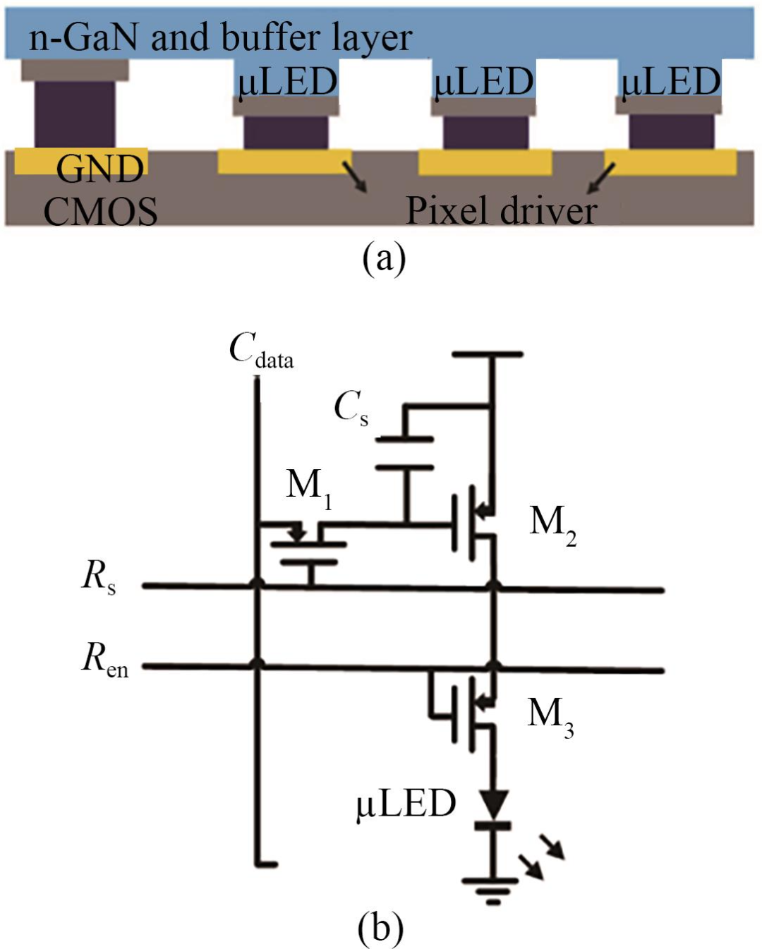
Figure 7: CMOS Driving. (a) Flip Bonding of Micro-LED Array and Active Matrix CMOS Backplane; (b) Pixel Driving Circuit Principle Diagram.
Source: Journal of the Society for Information Display, 2021, 29(1): 47-56.
French company Leti prepared CMOS driving circuit chips and bonded the CMOS driving chips with blue Micro-LED epitaxial layers. Then, through chip fabrication technology, blue Micro-LED arrays are made on the epitaxial layers, and the blue Micro-LED undergoes color conversion to obtain RGB Micro-LED unit groups. Using a micro-tube flip bonding method, the unit groups are integrated with the CMOS driving circuit units, creating a micro-integrated device composed of CMOS driving circuits and RGB Micro-LEDs. The entire device is transferred to a receiving substrate composed of row and column conductive lines, eliminating the need to transfer individual pixels sequentially to the receiving substrate, improving product yield. This method combines CMOS driving with a simple transfer process, producing Micro-LED displays with pixel unit sizes of 3 µm /5 µm. The fabrication process is shown in Figure 8.
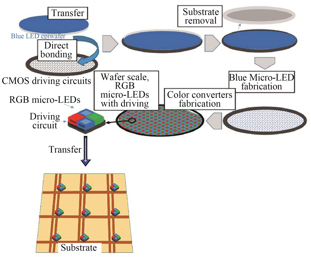
Figure 8: CMOS Driven RGB Micro-LED Display
Source: SID Symposium Digest of Technical Papers, 2019, 50(1): 240-243.
(2) TFT Driving Technology
TFT-driven Micro-LED display arrays are similar to traditional TFT-OLED technology, using bonding technology to transfer Micro-LED arrays to TFT-driven backplanes, with TFTs grown on glass substrates, primarily represented by amorphous silicon (a-Si) TFTs, low-temperature polycrystalline silicon (LTPS) TFTs, and oxide TFTs, as shown in Figure 9. a-Si TFTs have low carrier mobility, making them unsuitable for high-resolution displays and difficult to achieve high-quality displays. Currently, LTPS TFTs driven Micro-LED devices perform better due to their high carrier mobility, high integration, fast response speed, and low power consumption. LTPS TFTs can be integrated with the driving circuit process, providing good compatibility; however, they are more expensive than oxide TFTs. Oxide TFTs, mainly based on indium gallium zinc oxide (IGZO), have the advantages of low leakage current, fast response speed, and low fabrication cost, showing significant industrial prospects. An active LTPS/a-IGZO TFT driven Micro-LED array is shown in Figure 10.
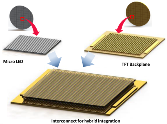
Figure 9: Integration of Micro-LED and TFT Driving Backplane
Source: SID Symposium Digest of Technical Papers, 2018, 49(1): 880-883.
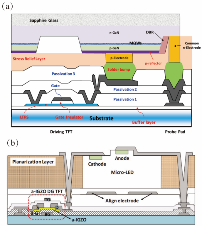
Figure 10: Schematic Diagram of Active TFT Driven Micro-LED Array
(a) Cross-sectional View of Dual-Gate a-IGZO TFT Driven Micro-LED Display
(b) Cross-sectional Structure Diagram of Micro-LED Array and LTPS TFT Driving
Source: (a) SID Symposium Digest of Technical Papers, 2020, 51(1): 335-338.
(b) SID Symposium Digest of Technical Papers, 2018, 49(1): 880-883.
Jin et al. from Kyung Hee University in South Korea proposed LTPO driving technology, combining p-type LTPS TFT and n-type IGZO TFT in a single pixel circuit. This pixel driving circuit has lower driving current and leakage current, reducing production costs and minimizing the impact of LTPS TFT self-heating effects, achieving high-resolution displays with better refresh stability, as shown in Figure 11.
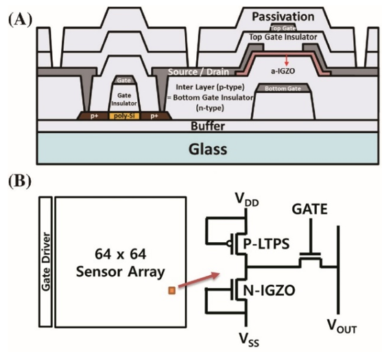
Figure 11: Cross-sectional View and Circuit Principle Diagram of LTPO TFT Driving Structure
Source: Journal of the Society for Information Display, 2020, 28(6): 528-534.
3. Summary and Outlook
Micro-LED can achieve fast response frequencies, high array integration, and high brightness transparent displays, showing potential in many display applications. Currently, the market for Micro-LED displays is still in its early stages, with no large-scale expansion, posing both opportunities and challenges for academia and industry. The small size of Micro-LED chips imposes stringent requirements on the driving thin film layers. The commonly used active driving methods are CMOS driving and TFT driving. By integrating the prepared Micro-LED chip arrays with CMOS/TFT driving using flip-chip bonding technology, the resulting Micro-LED displays can achieve high-performance image quality. When making Micro-LED into display devices, it is necessary to consider the various impacts of the small size of Micro-LED. Additionally, improving the efficiency and stability of the driver and Micro-LED array integration is also a current research direction. Furthermore, the Micro-LED industry chain is complex, and strict standards are required at all steps of Micro-LED display manufacturing, including chip fabrication, epitaxial growth, mass transfer, full-colorization, driving circuits, and panel manufacturing, with further breakthroughs needed in multiple technological areas.
Paper Information
Zhou Lu, Zheng Hua, Zhang Shenghao, Li Huadan, Zhang Geng, Zhang Shaoqiang, Xu Wei, Xu Hengrong, Xiao Junlin, Ning Honglong. Research Progress on Micro-LED Display and Its Driving Technology [J]. Liquid Crystal and Display, 2022, 37(11): 1395-1410.
https://cjlcd.lightpublishing.cn/thesisDetails#10.37188/CJLCD.2022-0157
Corresponding Author Introduction
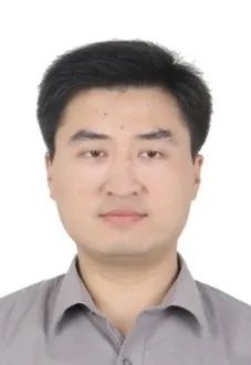
Zheng Hua, Associate Professor at Dongguan University of Technology, a backbone talent in the construction of high-level engineering and technology universities in Guangdong Province, a distinctive talent in Dongguan City, and the head of the Dongguan branch of the Guangdong Printing and Display Technology Innovation Alliance. He is an external master’s supervisor at South China Normal University and Guangdong University of Technology, and a visiting scholar at the Technical University of Dresden, Germany. He has been engaged in research in the flat panel display field for over 10 years, leading and participating in more than 10 national/provincial projects with research funding exceeding 4 million. He successfully developed the world’s first fully printed OLED display and published over 20 academic papers in internationally renowned journals such as Nature Communications. He previously served as the director of the R&D center at Shenzhen China Star Optoelectronics Technology Co., Ltd., holding 24 authorized Chinese invention patents, 21 US invention patents, and 1 invention patent each from Japan, South Korea, and Russia.
E-mail: [email protected]

Ning Honglong, PhD, Researcher, graduated from Tsinghua University in 2004. He has long been committed to the research of active information new-type display thin film transistor array materials and structures. He previously served as the chief scientist of Samsung Display Company in South Korea, a member of the Samsung Display Knowledge Property Patent Review Expert Group, and a certified Six Sigma Green Belt mentor at Samsung. In 2013, he returned to China and joined the State Key Laboratory of Luminescent Materials and Devices at South China University of Technology, focusing on new display material development, TFT unit and array structure design, flexible display device fabrication, printed display device fabrication, and performance optimization of information display devices. He has received the First Prize of Guangdong Province Science and Technology Invention Award in 2017 and the Second Prize of Guangdong Province Science and Technology Progress Award in 2021. He has led multiple national and provincial projects, including the National Key R&D Program, National Natural Science Foundation projects, and major scientific research plans in Guangdong Province. He has published over 200 papers and applied for over 200 patents, of which more than 100 have been authorized. He serves as a reviewer for academic journals such as ACS Appl. Mat. Interfaces, J. Mater. Chem. C, Ceram Int, IEEE Electr Device L, IEEE T Electron Dev, Soc. Inf. Display, and is an editorial board member of Liquid Crystal and Display and Digital Printing.
E-mail: [email protected]
Welcome to submit promotional articles for the research group
Please scan the QR code to contact the duty editor

banner promotionSupervised by: Zhang Ying, Zhao YangEdited by: Zhao Wei
Click here 👇 to follow me
Click[Looking], to receive our content updates in time