Source:Tiger Says Chip
Original Author:Tiger Says Chip
This article introduces the principles, structure, processes, and applications of NAND Flash.
Basic Principles and Structure of NAND Flash
What is NAND Flash?NAND Flash (flash memory) is a type of non-volatile memory technology primarily used for data storage. Unlike traditional DRAM or SRAM, NAND Flash retains data even when power is lost. It achieves data storage through the storage and release of charge.
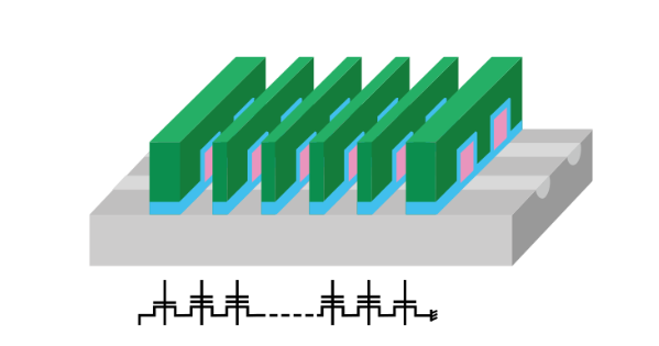
Figure:Arrangement structure of NAND Flash
Basic unit structure:The basic storage unit of NAND Flash is a Floating Gate Transistor. Each transistor corresponds to a storage unit, and the information stored is controlled by the charge on the floating gate. Multiple storage units are connected in series to form a NAND storage unit (typically 8 to 32 units in series) to increase density and reduce costs.
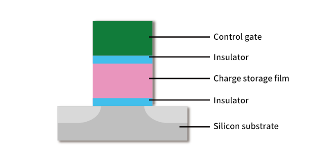
Figure: Device structure of storage cell
Working Principle of NAND Flash
Writing process (programming): During the programming (writing) process, a high voltage is applied, causing electrons to be injected into the floating gate, changing the charge on the floating gate, which in turn affects the conduction state of the transistor, representing different stored information (usually ‘0’ or ‘1’).
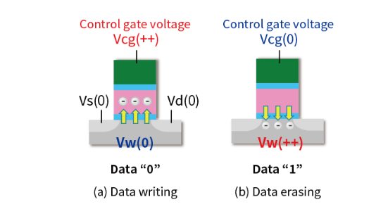
Figure: Data writing and erasing operations
Erasing process: NAND Flash uses a block erase method. By applying a reverse voltage, electrons on the floating gate are removed, restoring the transistor to its original state. Erasing typically operates on an entire block rather than a single byte.
Reading process: During the reading process, the charge state on the floating gate is detected to determine the conduction state of the storage unit, thus reading the stored information.
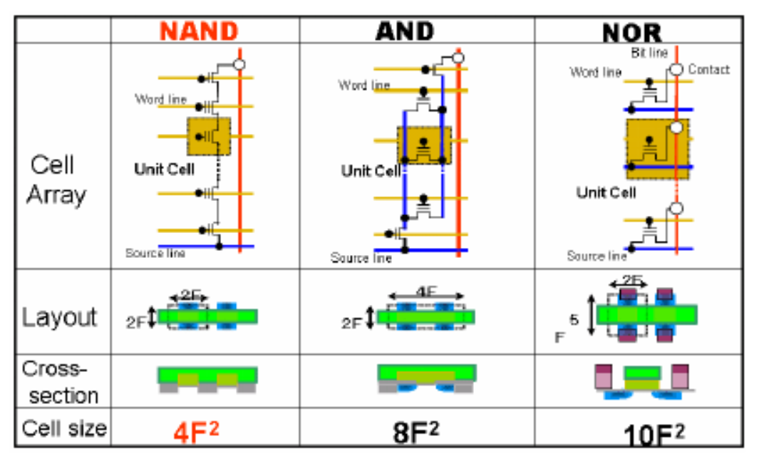
Figure: Representation of data 0 and data 1
Process and Technical Challenges of NAND Flash
Process node reduction: With technological advancements, the process nodes of NAND Flash continue to shrink (from 38nm to 19nm, and even smaller nodes), resulting in higher storage density and lower costs, but also increasing manufacturing complexity and yield challenges.
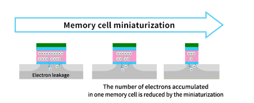
Figure: Trend of storage cell miniaturization
Reliability optimization: As the size of storage units decreases, the stability of charge storage declines, leading to reduced durability and data retention time. To address this issue, engineers need to continuously optimize process parameters to enhance reliability. For example, increasing the number of erase cycles (such as 500K cycles for 38nm technology) can improve durability.
Design rule shrinkage and layout optimization: At smaller process nodes, design rules need to be continuously reduced, and layouts need to be optimized to achieve more storage units in a smaller space. Reducing masks and optimizing rules are important means to improve yield and reduce costs.
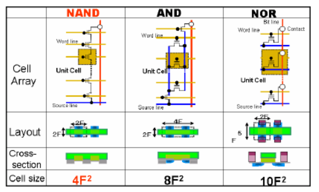
Figure: Comparison of NAND, AND, and NOR cell arrays
Applications and Development Trends of NAND Flash
Application fields: NAND Flash is widely used in various storage devices, such as solid-state drives (SSD), USB flash drives, and memory cards. It is also extensively used in smartphones, tablets, and servers.
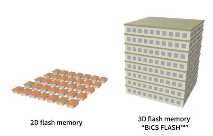
Figure: Structural details of 3D NAND
3D NAND technology: As the difficulties of shrinking the two-dimensional plane increase, 3D NAND technology has emerged. 3D NAND significantly increases storage density by vertically stacking storage units, becoming the main direction of NAND Flash development.
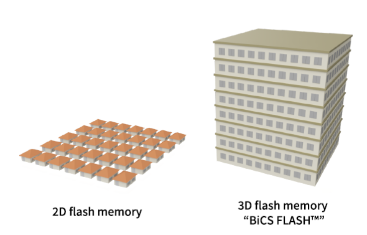
Figure: Conceptual comparison of 2D Flash and 3D Flash
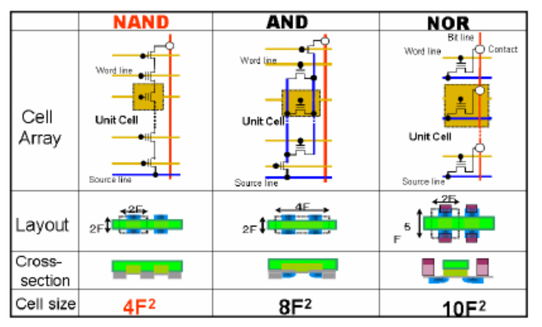
Figure: Comparison of device structures of 2D Flash and 3D Flash
Future Challenges and Outlook
Further improvements in reliability and durability: As storage units continue to shrink, future reliability challenges will increase. New materials and structural innovations may be key to solving this issue.
Competition from new storage technologies: With the development of new storage technologies (such as ReRAM, MRAM, etc.), NAND Flash will face new competition, and continuous process innovation and cost optimization will be key to maintaining competitiveness.
END
The reproduced content only represents the author’s views
It does not represent the position of the Semiconductor Research Institute of the Chinese Academy of Sciences
Editor: Silence
Responsible Editor: Catnip
Submission Email: [email protected]
Previous Recommendations
1. The Semiconductor Institute has made a series of progress in low-dimensional semiconductor polarization light detection
2. From a physics rising star to a pioneer in Chinese semiconductors | History of Science and Technology
3. The Semiconductor Institute has been approved as a “Beijing International Science and Technology Cooperation Base”
4. The Semiconductor Institute’s collective guided mode resonance chiral laser research has made progress
5. The team of Zhu Lijun from the Semiconductor Institute and collaborators have made important research progress in the physical origin of anomalous magnetoresistance in magnetic heterojunctions
6. The optical fiber sensing team of the Semiconductor Institute has contributed to the successful convening of the 2025 Disaster Prevention and Mitigation Conference