In Silicon Valley Legend I:
Shockley and the Transistor, we told the story of the birth of the transistor and Shockley’s journey to Silicon Valley to start a business, as well as the origins of Fairchild Semiconductor. We also introduced how this pioneering company obtained funding, intertwined with the enmity between Shockley and others. In the second part of the Silicon Valley Legend series, we will explore the development of planar technology, outline the “genealogy” of many semiconductor startups (Fairchildren) derived from Fairchild Semiconductor, and discuss the competition between Intel and Texas Instruments in integrated circuits.
Fairchild Semiconductor
Fairchild Semiconductor opened at 844 East Charleston Road, located at the intersection of Mountain View and Palo Alto. Fairchild displayed remarkable innovation, creating important technologies that influenced the world in the second half of the 20th century. With the successful development of planar silicon transistors, Fairchild Semiconductor quickly grew into a leader in the semiconductor industry.
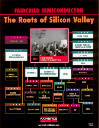
Fairchild Semiconductor genealogy (Image source: Fairchild Semiconductors)
Although transistors were very successful, they faced a new challenge known as “digital tyranny” (Wikipedia: Digital tyranny was a problem faced by computer engineers in the 1960s. Due to the large number of components involved, engineers could not improve the performance of their designs. Theoretically, each component needed to be connected to others, often manually wired and soldered. To improve performance, more components would be needed). If you wanted to make a simple flip-flop, you needed four transistors and about ten wires to connect them. Interconnecting two flip-flops required not only double the transistors but also four to five additional wires to connect them. In this way, 4 transistors required 10 wires, 8 required 25 wires, and 16 required 60 to 70 wires. In other words, as the number of transistors increased linearly, the number of connections grew exponentially (an exponent between 1 and 2).
While mass-producing transistors is relatively straightforward, connecting them is much more difficult because wires must be soldered together manually, which takes up a lot of space. The desire to build larger and more complex systems was thus hindered. At that time, few people paid attention to wiring, but connections quickly became a potential bottleneck, leading to the demand for integrated circuits.
Planar Technology
In 1958, Jack Kilby of Texas Instruments demonstrated how to integrate a pair of transistors on a semiconductor substrate. At that time, Texas Instruments was a competitor of Fairchild Semiconductor, and Kilby’s transistors were wire-bonded, which did not solve the connection problem. Ultimately, the connection issue was resolved by Bob Noyce with the help of Jean Hoerni and Jay Last.
Hoerni had been researching ways to reduce transistor defects and found that defects stemmed from the unprotected surface of transistors inside the package, which became contaminated over time, leading to performance degradation. His solution was to grow or deposit a layer of silicon dioxide (SiO2) on top of the transistor structure to form a passivation layer or protective layer, thus protecting the transistor surface from contamination. Unlike the mesa process (where the emitter and base are deposited on top of the substrate), Hoerni’s idea was that if the surface was completely covered with silicon dioxide, the regions of the emitter and base could be selectively diffused, resulting in a smoother surface that allowed for greater automation in the transistor manufacturing process.
This technology, announced in January 1959, became the second most important invention in the history of microelectronics—second only to the invention of the transistor—and laid the groundwork for the later invention of integrated circuits. At the time, this great invention received little attention, except from Noyce, who realized that the glass layer was an insulator, allowing for the creation of a connection layer placed on top, similar to the patterns on printed circuit boards.
Noyce filed a patent in April 1959, which then led to a legal dispute between Texas Instruments and Fairchild Semiconductor (at that time, Kilby and Noyce were still friends and held each other in high regard). Texas Instruments claimed that Kilby’s patent statement—”a method of laying conductive materials such as gold on insulating materials to establish necessary connections”—preceded Noyce’s patent statement, and Kilby’s patent used simple wire bonding to connect wires, which was the quickest modeling method. If Texas Instruments’ patent was recognized, then Noyce’s patent would be declared invalid.
Ultimately, Texas Instruments lost the case, both patents were declared valid, and the two companies reached a cross-licensing agreement.
Kilby was naturally a very humble person, and although his patent was announced before Noyce’s, he generously declared that both he and Noyce were inventors of the integrated circuit, despite this being contrary to the position of Texas Instruments’ management. In 1959, Sherman Fairchild exercised his right to purchase shares from the founding members, turning the original founding partners into ordinary employees, undermining the company’s team spirit and sowing the seeds for future divisions.
How to prevent interference between adjacent transistors was another major issue as integrated circuits entered the commercialization phase. Noyce entrusted this tricky problem to Jay Last, who was responsible for the R&D team. However, it was not an easy task, taking about 18 months before the first functional device was developed on September 27, 1960.
Fairchild’s Troubles
At this time, there was also significant internal resistance in the development of integrated circuits, with Fairchild’s Vice President of Marketing Tom Bay accusing Last of wasting resources. In November 1960, Tom Bay requested to terminate this R&D project and redirect the saved money to transistor development. At this point, Moore refused to help, and Noyce also avoided discussing the matter, leaving Last to fight on his own. Just one month after Fairchild announced the shift of its transistor production from mesa technology to planar technology, internal conflicts erupted. Moore refused to credit this achievement to Hoerni, further exacerbating the already tense relations among the eight founding partners.
Jay Last continued to develop six devices, but the ongoing conflicts became the last straw. With the success of planar technology and isolation technology, Last and Hoerni left Fairchild on January 31, 1961. With funding arranged by Arthur Rock at Teledyne, they founded Amelco in Mountain View to develop integrated circuit devices to support Teledyne’s military business. A few weeks later, Eugene Kleiner and Sheldon Roberts joined this new company. Due to this core team’s split, the eight founding members divided into two factions.
In March 1961, Fairchild announced the launch of the world’s first standard logic integrated circuit series, namely the direct-coupled transistor logic device. This device adopted the resistor-transistor logic (RTL) planar technology developed by Hoerni and Last, but was registered under the µLogic trademark. The µL903 device in this series is a 3-input NOR gate, which became a fundamental component of the guidance computer in the Apollo lunar program. This lunar navigation computer was designed by MIT, manufactured by Raytheon, and integrated 5000 devices, marking the first major application of ICs. This miniaturization for space applications propelled the early development of integrated circuits.
However, Fairchild’s leading advantage was short-lived. As Hoerni and Last left, David Ellison, Lionel Catania, and others also departed, founding Signetics. A year later, in 1962, this company released the significantly improved second-generation logic series, the SE100 series diode-transistor logic (DTL) chips. Fairchild quickly retaliated with its own 930 series DTL devices, thereby weakening Signetics’ strength and rendering it unable to compete with Fairchild in the market.
NE555 Timer: The Most Popular IC?
Signetics’ most famous chip is the NE555 timer, released in 1971, which, along with the ubiquitous TTL 7400 quad 2-input NAND gate chip, became one of the most popular integrated circuit devices of all time. Signetics was acquired by Philips in 1975.
Early chips mainly used TO-5 or TO-18 metal can transistor packages, which worked well for three-lead devices but struggled to provide more connections due to the size limitation of their packaging, with radial leads arranged as densely as possible. Ten leads were the practical limit, and they could not support more complex ICs. In 1964, Don Forbes, Rex Rice, and Bryant Rogers of Fairchild invented the now-familiar dual in-line package, solving this issue. For the next 40 years, this tiny “millipede” would “crawl” across circuit boards.
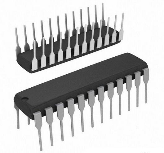
Dual in-line package (Image source: Google)
This packaging technology originated in 1962, designed by Texas Instruments engineer Yung Tao, and later became the industry standard for surface mount integrated circuits for the U.S. military. This concept applied to through-hole PCB installations aimed to facilitate operations for electronic manufacturers and simplify PCB layout design. This approach made it easier to power the increasing number of ICs and allowed for more inputs and outputs on the circuit board. Another consideration was cost, as the consumer IC device market was rapidly growing. The 0.1-inch lead spacing allowed enough space for PCB wiring between leads, while a lead pitch of 0.3 inches left space for other components.
Fairchild introduced the dual in-line package in 1965, initially using ceramic materials. However, when Texas Instruments launched plastic resin packaging, this packaging method rapidly developed, significantly reducing unit costs. Due to excellent design, low cost, and support for increasingly complex integrated circuits, plastic dual in-line packaging became the industry standard, with its basic 14-lead design expanded to support more leads, reaching up to 64 leads in a 0.6-inch wide footprint. As integrated circuits evolved, the complexity and lead requirements of chips eventually exceeded the capabilities of dual in-line packaging, leading to its obsolescence in the late 20th century, replaced by the second generation of surface mount devices (e.g., BGA).
With up to 15,000 bare chips per wafer, the cost of packaging and testing far exceeded that of the wafer, necessitating lower labor costs for continued development. Early wafer fabs undertook many labor-reducing measures, such as employing low-cost Native Americans in the Navajo Reservation in New Mexico and early automation attempts. After many failures, it was ultimately proven successful to outsource testing and packaging to Asia, at least in the short term. At that time, Bob Noyce invested in a small radio company in Hong Kong and suggested Charlie Sporck and Jerry Levine to explore the area.
Sporck and Levine were attracted by the low labor costs, absence of union organizations, Western-educated technicians, quality engineering schools, as well as tax incentives and other government subsidies. In 1963, Fairchild Semiconductor established its first Far East packaging and testing plant in a former shoe factory on the Kowloon side of Hong Kong. Other semiconductor manufacturers soon followed Fairchild to the Far East, primarily to places like Malaysia.
From Motels to Intel
Blank, Greenwich, Moore, and Noyce stayed at Fairchild until 1968. In March of that year, Moore and Noyce decided to leave, seeking financing from Arthur Rock, and founded NM Electronics in the summer of 1968. A year later, NM Electronics purchased the naming rights from the motel chain Intelco, thus founding Intel.
Greenwich also left Fairchild in 1968, first teaching at UC-Berkeley and Stanford, during which he published the first comprehensive textbook on integrated circuits. However, Greenwich never lost his entrepreneurial spirit, and he left academia in 1985 to co-found and run several startups, including the industrial RFID tag developer Escort Memory Systems.
Blank was the last of the eight defectors, ultimately leaving Fairchild in 1969 to become a consultant for tech startups. Seeking to do something more practical, he co-founded Xicor in 1978, producing electrically erasable programmable read-only memory (EEPROM).
As for the other four “defectors,” Hoerni continued to manage Amelco until the summer of 1963, when he left after a conflict with Teledyne’s owner, moving to Union Carbide Electronics. In July 1967, with support from the Swatch Group’s predecessor, SSIH, he founded Intersil, which pioneered the low-power custom CMOS circuit market, some of which were developed for Seiko, thus spurring the boom of the Japanese electronic watch industry.
Hoerni then launched Eurosil, the European version of Intersil, as SSIH sought to establish a plant near Munich, not far from the Swiss watch manufacturing base, thus participating in partial investment. Eurosil was eventually sold to Diehl at the end of 1975. Hoerni left there in 1980, returning to the West Coast of California and founding a startup named Telmos, which produced semi-custom products covering linear interfaces between sensors and microprocessors, digital logic cores, and high-voltage and high-current drivers.
Jay Last continued to work at Amelco, serving as Vice President of Technology at Teledyne’s parent company for 12 years. In 1982, he founded Hillcrest Publishing, specializing in publishing art books. Roberts also left to start his own business and later served as a trustee at Rensselaer Polytechnic Institute.
At this point, only Kleiner remained, who eventually also left to pursue a career financing many startups emerging on the West Coast. He collaborated with HP’s R&D head Thomas Perkins to establish the venture capital firm Kleiner Perkins. They opened an office on Dune Road in Palo Alto, which became a holy site for American venture capitalists. While Arthur Rock and Hayden Stone could be considered pioneers of venture capital firms, Kleiner Perkins was the first to have a physical office in Silicon Valley.
This VC firm invested in Amazon, Compaq, Genentech, Intuit, Lotus, Macromedia, Netscape, Sun Microsystems, Symantec, and dozens of other startups.
Today, as the first company derived from Fairchild, Amelco has ceased to exist after multiple mergers, acquisitions, and transformations, but its core technologies and intellectual property still exist, now owned by Microchip.
The storied Fairchild Semiconductor itself was acquired by ON Semiconductor in 2016, thus becoming a permanent legend.
(The second part of the Silicon Valley Legend series introduces the separation of the eight founders of Fairchild and their respective fates, with nearly all well-known semiconductor companies having some connection to Fairchild. In the third part, we will delve into Silicon Valley’s high-tech tradition and the three inventions that changed the world—integrated circuits, startups, and venture capital.)