The RK3588 DDR controller interface supports the JEDEC SDRAM standard interface. The schematic circuit for 16-bit data signals is shown in Figure 8-1, address and control signals are shown in Figure 8-2, and power signals are shown in Figure 8-3. The circuit controller has the following characteristics:
1. Compatible with LPDDR4/LPDDR4X/LPDDR5 standards;
2. Supports a 64-bit data bus width, composed of 4 channels of 16 bits each, with a maximum addressable capacity of 8GB per channel; the total capacity can reach 32GB with 4 channels;
3. Two 16-bit channels form one 32-bit channel; the two 32-bit channels (i.e., CH0 and CH1 in the schematic) cannot use different capacity configurations, such as 4GB + 2GB;
4. Supports Power Down, Self Refresh, and other modes;
5. Features programmable output with dynamic PVT compensation and ODT impedance adjustment.
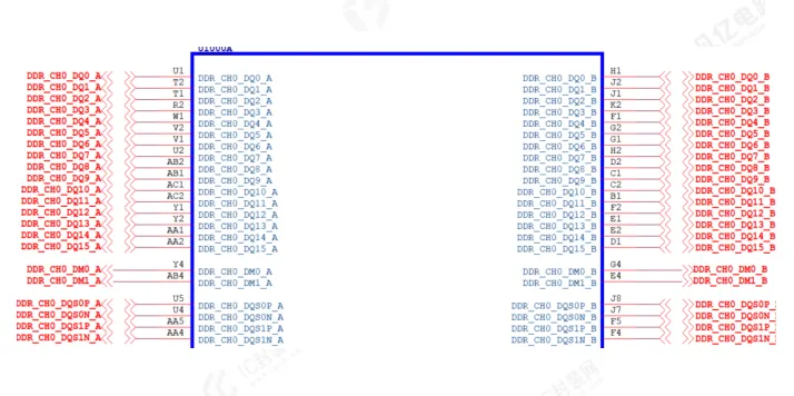
Figure 8-1 RK3588 DDR Data Signal Pins
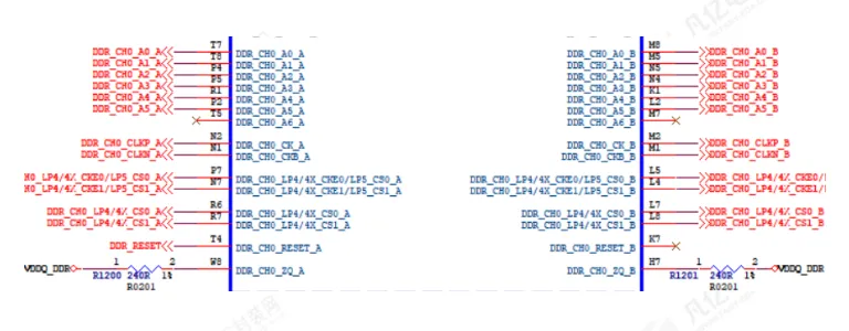
Figure 8-2 RK3588 DDR Address and Control Signal Pins
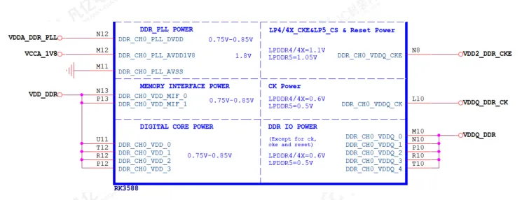
Figure 8-3 RK3588 DDR Power Pins
1. Ensure the schematic of RK3588 DDR PHY and each DRAM chip maintains consistency with the original design from Rockchip, including decoupling capacitors for DDR power sections;
2. RK3588 supports LPDDR4/LPDDR4X, LPDDR5, which have different I/O signals; select corresponding signals based on the DRAM type;
3. DQ and CA sequences must not be swapped; if PCB routing needs to adjust pins, communicate with Rockchip’s original FAE;
4. ZQ of LPDDR4/4X chips must be connected to VDDQ_DDR_S0 power with a 240-ohm 1% resistor;
5. ODT_CA of LPDDR4/4X chips must be connected to VDD2_DDR_S3 power with a 10K-ohm 5% resistor;
6. The built-in Retention function requires that during the self-refresh period of DDR, the power pin DDR_CH_VDDQ_CKE of the DDR controller must maintain power supply, while other power supplies can be turned off; the VDDQ power of DDR chips can be turned off 5ns after tCKELCK, while other power supplies cannot be turned off;
7. LPDDR5 introduces WCK clock; there are two operating clocks for LPDDR5, one is CK_t and CK_c for controlling command and address operations, and the other is WCK_t and WCK_c, where WCK can run at 2x or 4x the CK frequency; during Write, WCK serves as both clock and Write data strobe; during Read, WCK serves as the clock for DQ and RDQS, where RDQS is the Read data strobe signal;
8. RK3588 supports DVFSC Mode (when running LPDDR5), which allows switching between VDD2L (0.9V) and VDD2H (1.05V); high-frequency operations use VDD2H voltage, while low-frequency operations use VDD2L voltage.
1. When using 2 LPDDR4/4x chips at 32 bits, DQ and CA adopt a point-to-point topology, as shown in Figure 8-4, with matching for LPDDR4 chips DQ, CLK, CMD, CA all supporting ODT, all connected point-to-point;
2. When using 2 LPDDR5 chips at 32 bits, DQ and CA adopt a point-to-point topology, as shown in Figure 8-5, with matching for LPDDR5 chips DQ, CLK, CMD, CA all supporting ODT, all connected point-to-point.
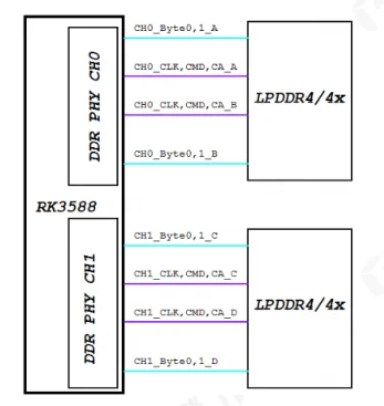
Figure 8-4 LPDDR4 Point-to-Point Topology
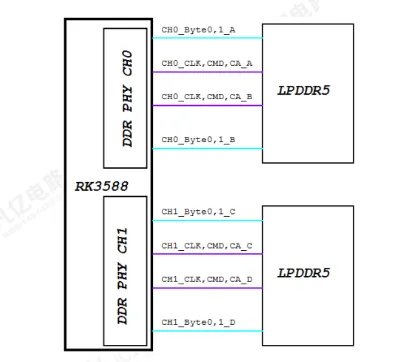
Figure 8-5 LPDDR5 Point-to-Point Topology
1. The power supply summary for RK3588 DDR PHY is shown in Table 8-1:
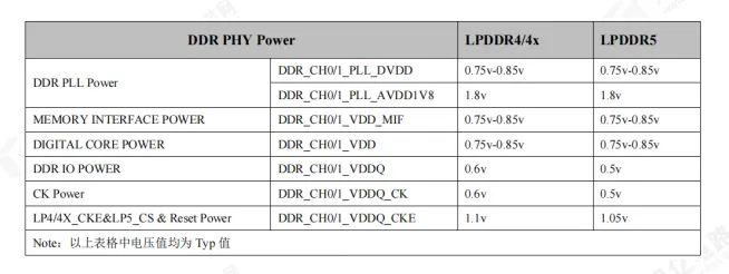
Table 8-1 RK3588 DDR PHY Power Supply
2. The power supply summary for LPDDR4/4x/LPDDR5 chips is shown in Table 8-2:
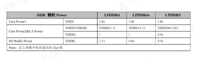
Table 8-2 Power Supply for LPDDR4/4x/LPDDR5
1. Power Supply Circuit When Using Dual PMIC Power Solution
1.1 Use Rockchip’s compatible PMIC model RK806-2; be sure to adjust the feedback resistor value of PMIC2 RK806-2 FB9 (pin 66) according to the actual DRAM chips used, so that the output voltage of VDDQ_DDR_S0 matches the chip, as shown in Figure 8-6;
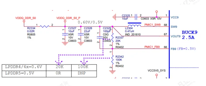
Figure 8-6 RK806-2 BUCK9 FB Parameter Adjustment
1.2 Use Rockchip’s compatible PMIC model RK806-2; be sure to adjust the feedback resistor value of PMIC2 RK806-2 FB9 (pin 66) according to the actual DRAM chips used, so that the output voltage of VDD2_DDR_S3 matches the chip, as shown in Figure 8-7;
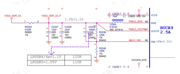
Figure 8-7 RK806-2 BUCK9 FB Parameter Adjustment
2. Power Supply Circuit When Using Single PMIC Power Solution
1. Use Rockchip’s compatible PMIC model RK806-1; be sure to adjust the feedback resistor value of PMIC RK806-1 FB9 (pin 66) according to the actual DRAM chips used, so that the output voltage of VDDQ_DDR_S0 matches the chip, as shown in Figure 8-8;
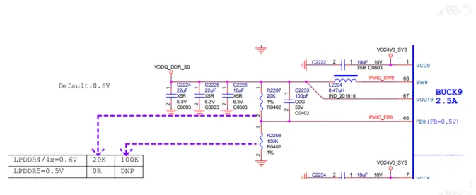
Figure 8-8 RK806-1 BUCK9 FB Parameter Adjustment
2. Use Rockchip’s compatible PMIC model RK806-1; be sure to adjust the feedback resistor value of PMIC RK806-1 FB6 (pin 31) according to the actual DRAM chips used, so that the output voltage of VDD2_DDR_S3 matches the chip, as shown in Figure 8-9;
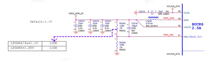
Figure 8-9 RK806-1 BUCK6 FB Parameter Adjustment
3. The original RK3588 circuit schematic reference template provided by Rockchip includes compatibility designs for LPDDR4 and LPDDR4X. It is important to select the appropriate circuit based on the actual materials used. When using LPDDR4 chips, only R3811 resistor should be used; when using LPDDR4X chips, only R3808 resistor should be used, as shown in Figure 8-10.
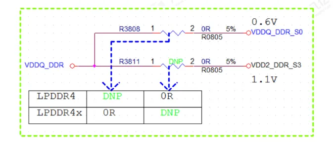
Figure 8-10 LPDDR4/LPDDR4X Compatibility Design Power Selection
8-Layer Through-Hole Board 1.6mm Thickness Layering and Impedance Design
In the 8-layer through-hole board layering design, the reference plane for the top layer signal L1 is L2, and the reference plane for the bottom layer signal L8 is L7. The suggested layering is TOP-Gnd-Signal-Power-Gnd-Signal-Gnd-Bottom, with a recommended copper thickness of 1oz, and a total thickness of 1.6mm. The detailed layering and impedance design process can be found in Chapter 2 of the white paper. The recommended board thickness layering is shown in Figure 8-11, and the impedance line width and spacing are shown in Figure 8-12.
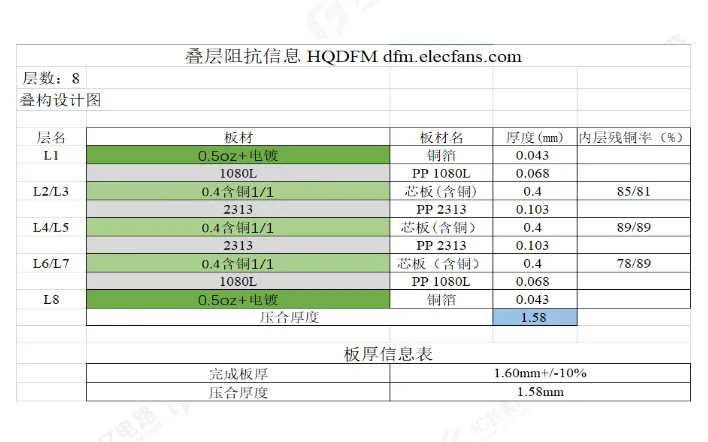
Figure 8-11 Recommended Layering for 8-Layer Through-Hole 1.6mm Thickness
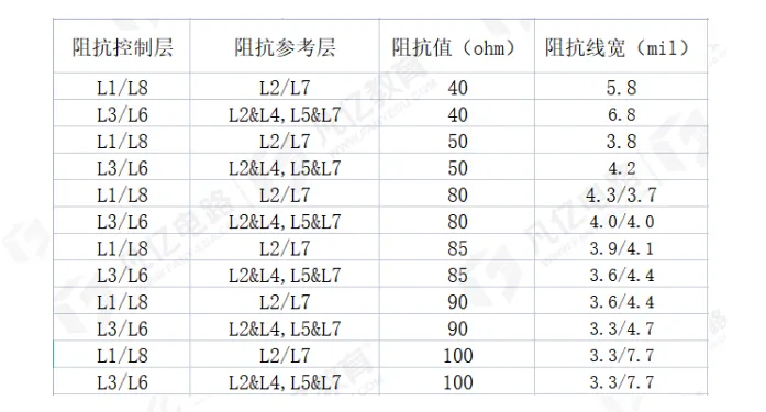
Figure 8-12 8-Layer Through-Hole 1.6mm Thickness Impedance Line Width and Spacing
10-Layer First-Order HDI Board 1.6mm Thickness Layering and Impedance Design
In the 10-layer first-order board layering design, the reference plane for the top layer signal L1 is L2, and the reference plane for the bottom layer signal L10 is L9. The suggested layering is TOP-Signal/Gnd-Gnd/Power-Signal-Gnd/Power-Gnd/Power-Signal-Gnd-Bottom, where L1, L2, L9, and L10 are recommended to use 1oz, and other inner layers use HoZ. The detailed layering and impedance design process can be found in Chapter 2 of the white paper. The recommended board thickness layering is shown in Figure 8-13, and the impedance line width and spacing are shown in Figure 8-14.
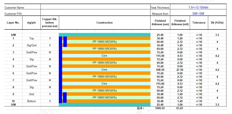
Figure 8-13 10-Layer First-Order HDI Board Layering Design

Figure 8-14 10-Layer First-Order HDI Board Impedance Design
10-Layer Second-Order HDI Board 1.6mm Thickness Layering and Impedance Design
In the 10-layer second-order board layering design, the reference plane for the top layer signal L1 is L2, and the reference plane for the bottom layer signal L10 is L9. The suggested layering is TOP-Gnd-Signal-Gnd-Power-Signal/Power-Gnd-Signal-Gnd-Bottom, where L1, L2, L3, L8, L9, and L10 are recommended to use 1oz, and other inner layers use HoZ. The detailed layering and impedance design process can be found in Chapter 2 of the white paper. The recommended board thickness layering is shown in Figure 8-15, and the impedance line width and spacing are shown in Figures 8-16 and 8-17.

Figure 8-15 10-Layer Second-Order HDI Board Layering Design

Figure 8-16 10-Layer Second-Order HDI Board Single-Ended Impedance Design
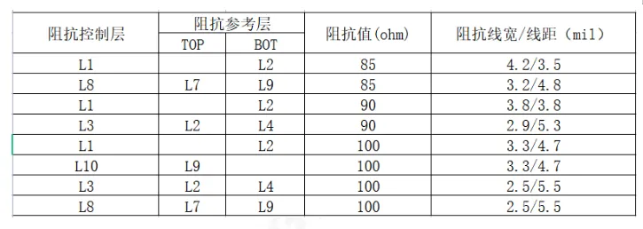
Figure 8-17 10-Layer Second-Order HDI Board Differential Impedance Design
1. All channel data DQ and DM single-ended signal impedance should be 40 ohms; if the layering cannot meet the target impedance of 40 ohms, ensure at least that the impedance meets 45 ohms ±10%. The target impedance of 40 ohms will have a larger signal margin, while 45 ohms will have a smaller signal margin, as shown in Figure 8-18;
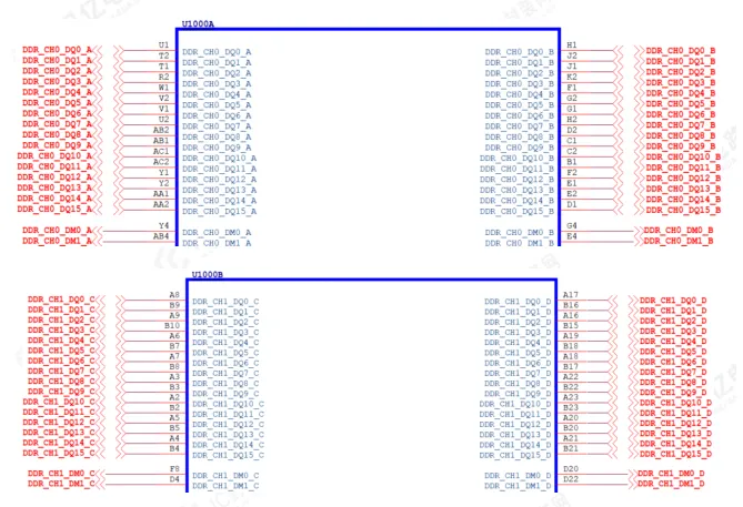
Figure 8-18 CH0 and CH1 Channel Data DQ and DM Impedance Lines
2. All channel address and control single-ended signal impedance should be 40 ohms, as shown in Figure 8-19;
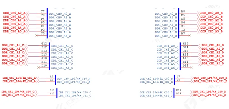
Figure 8-19 CH0 and CH1 Channel Address and Control Impedance Lines
3. CKE single-ended signal impedance should be 50 ohms, as shown in Figure 8-20;
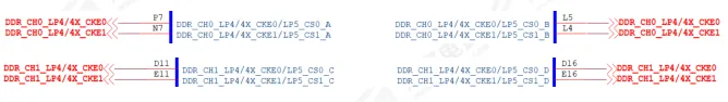
Figure 8-20 CH0 and CH1 Channel CKE Impedance Lines
4. All channel data latch signals DQS and clock differential signals should have an impedance of 80 ohms; if the layering cannot meet the target impedance of 80 ohms, ensure at least that the impedance meets 90 ohms ±10%, as shown in Figure 8-21;
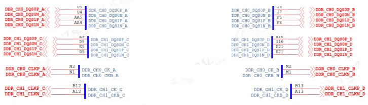
Figure 8-21 CH0 and CH1 Channel DQS and CLK Differential Impedance Lines
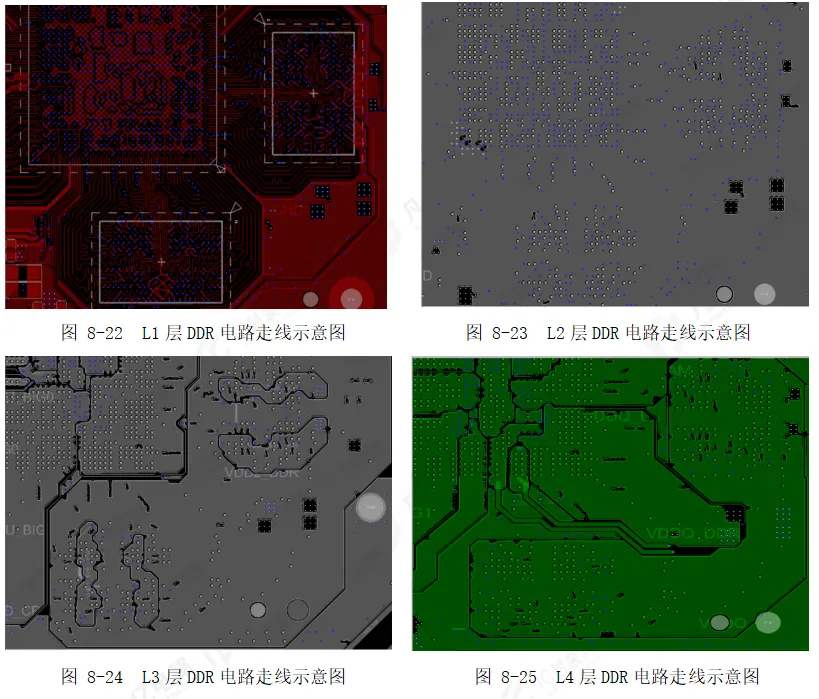
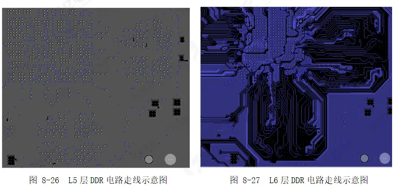
1. Since the RK3588 DDR interface speed can reach up to 4266Mbps, the difficulty of PCB design is high. Therefore, it is strongly recommended to use the DDR templates and corresponding DDR firmware provided by Rockchip. The DDR templates are released after strict simulation and testing validation. If there is enough space in the single-board PCB design, prioritize leaving layout and wiring space required for the DDR circuit module, and copy the DDR templates provided by Rockchip, ensuring that the relative positions of the chip and DDR chips, power filtering capacitor positions, copper pouring spacing, etc., are all consistent as shown in Figures 8-22 to 8-29.
2. If you design the PCB yourself, please refer to the following PCB design recommendations. It is strongly recommended to perform simulation optimization and then confirm with Rockchip’s original FAE before proceeding with prototyping and debugging.
-
For CPU pins, the corresponding number of GND vias should strictly follow the template design, and GND vias cannot be reduced. The GND via design for CPU pins in the 8-layer through-hole PCB template is shown in Figure 8-30, with yellow indicating DDR signal pins and red indicating ground pins;
Figure 8-30 RK3588 Ground Via Schematic
-
When changing layers for signals, if the reference layers are all GND planes, GND return vias need to be added within a distance of 25mil (center-to-center distance between vias) around the signal via (yellow for DDR signals, red for GND signals) to improve the signal return path. Each signal via should have at least one GND return via, and increasing the number of GND return vias can further improve signal quality, as shown in Figure 8-31;
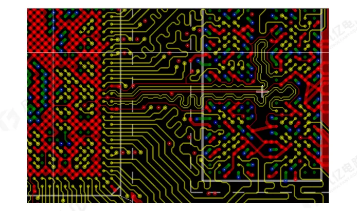
Figure 8-31 Signal Layer Change Adding Ground Via Schematic
-
The position of GND vias and signal vias will affect signal quality. It is recommended to place GND vias and signal vias in an interleaved manner as shown in Figure 8-32. Although there are 4 GND return vias, avoid placing 4 signal vias together, as this will maximize the crosstalk between vias;
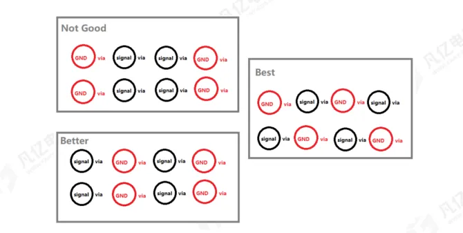
Figure 8-32 Ground Return Via Position Schematic
-
For 8-layer boards, it is recommended that DDR signals run on the first, sixth, and eighth layers. DQ, DQS, address and control signals, and CLK signals should all reference a complete GND plane. If the GND plane is incomplete, it will greatly affect signal quality;
-
As shown in Figure 8-33, when vias cause the signal reference layer to break, consider using GND routing to optimize the reference layer and improve signal quality;
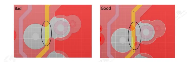
Figure 8-33 Ground Plane Breakage Repair Schematic
-
Signal crosstalk can affect signal delay; when routing, be mindful of equal length as shown in Figure 8-34;
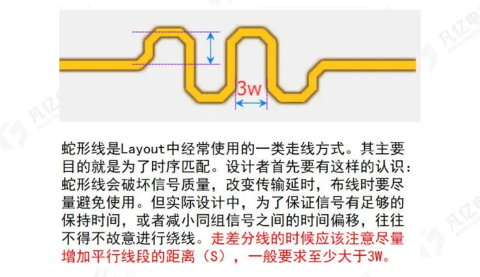
Figure 8-34 S-shaped Routing Schematic
-
When equal lengths are made, consider the delay caused by vias, as shown in Figure 8-35;
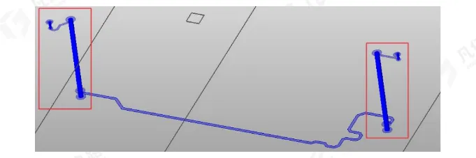
Figure 8-35 Via Delay Schematic
-
Non-functional pads can damage copper foil and increase the parasitic capacitance of vias; it is necessary to delete non-functional pads from vias and design without pads;
-
The closer the routing distance to the via, the poorer the reference plane; the routing distance to the via should be >=8mil, and increase the spacing wherever possible;
-
Adjust the position of vias to optimize the cracks in the plane, avoiding plane breakage and improving return paths, as shown in Figure 8-36;
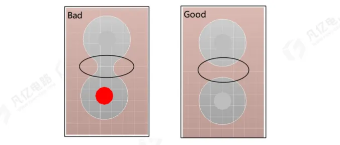
Figure 8-36 Via Optimization Schematic
-
DQS, CLK, and WCLK signals need to be ground-wrapped; it is recommended to place a GND via every 400mil or less along the ground wrap line or copper foil, as shown in Figure 8-37;
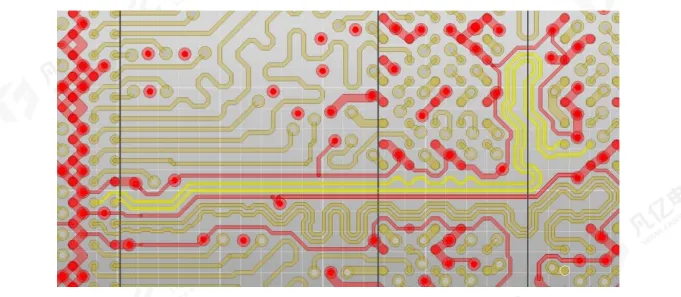
Figure 8-37 Differential Signal Ground Wrap Schematic
-
For the VDD_DDR power supply, when changing layers in the DCDC area, it is recommended to use >=6 0503 vias;
-
For the VDDQ_DDR power supply, when changing layers in the DCDC area, it is recommended to use >=6 0503 vias;
-
For the VDD2_DDR power supply, when changing layers in the DCDC area, it is recommended to use >=6 0503 vias;
-
For the VDD1_1V8_DDR power supply, when changing layers in the power plane, it is recommended to use at least >=2 0402 vias;
-
Each capacitor pad is recommended to have at least one via; for capacitors in 0603 or 0805 packages, it is recommended that one pad corresponds to two vias, with the vias placed close to the pins to reduce loop inductance.
Due to the 8-layer board, there are traces on both the outer and inner layers. Whether single-ended signals or differential signals, there are differences in speed between traces on the outer layer and traces on the inner layer. For outer layer traces, there are differences in speed for single-ended and differential signals. For inner layer traces, the differences between single-ended and differential signals are smaller. The speed of vias also differs from that of traces; to reduce the impact of speed differences on signal margins, design rules need to be set according to equal delay. When designing the PCB, the layering parameters should be set according to the actual board fabrication while considering package delay and via delay. The specific timing requirements are shown in Table 8-3.
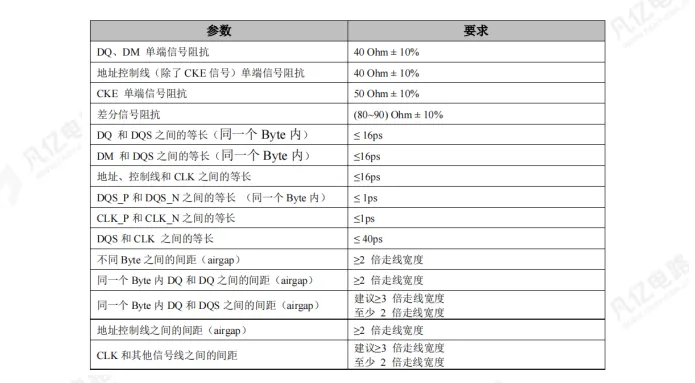
Table 8-3 LPDDR4 Impedance and Timing Table