In our daily lives, the USB drives, TF cards, SD cards, and DDR memory and SSDs used in computers all belong to a storage technology known as “semiconductor storage”.
Let’s get straight to the point with a complete classification diagram of semiconductor storage:
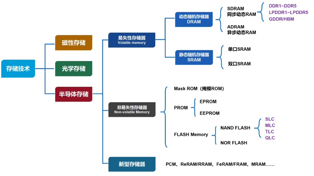
Today, I will focus on sharing knowledge in this area.
Classification of Semiconductor Storage
Modern storage technology can be broadly divided into three major parts: magnetic storage, optical storage, and semiconductor storage.
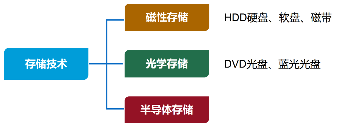
In simple terms, semiconductor memory refers to memory that uses “semiconductor integrated circuits” as the storage medium.
If you disassemble your USB drive or SSD, you will find PCB circuit boards, along with various chips and components. Among them, there is a type of chip specifically designed for data storage, sometimes referred to as a “storage chip”.
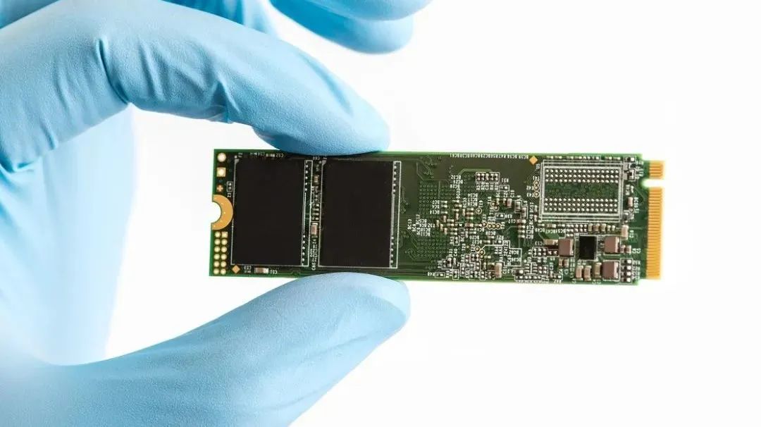
Compared to traditional disks (such as HDDs), semiconductor memory is lighter, smaller, and faster in read/write speeds. Of course, it is also more expensive.
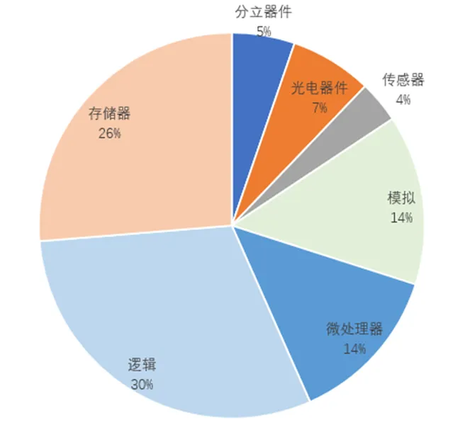
In recent years, there has been a high level of attention on the semiconductor chip industry. However, most of the focus has been on computing chips like CPUs, GPUs, and mobile SoCs.
What many do not realize is that semiconductor memory is also one of the core pillars of the entire semiconductor industry. In 2021, the global market size for semiconductor memory was $153.8 billion, accounting for 33% of the entire integrated circuit market, which is one-third.
Semiconductor memory is also a large category that can be further divided mainly into: volatile (VM) memory and non-volatile (NVM) memory.
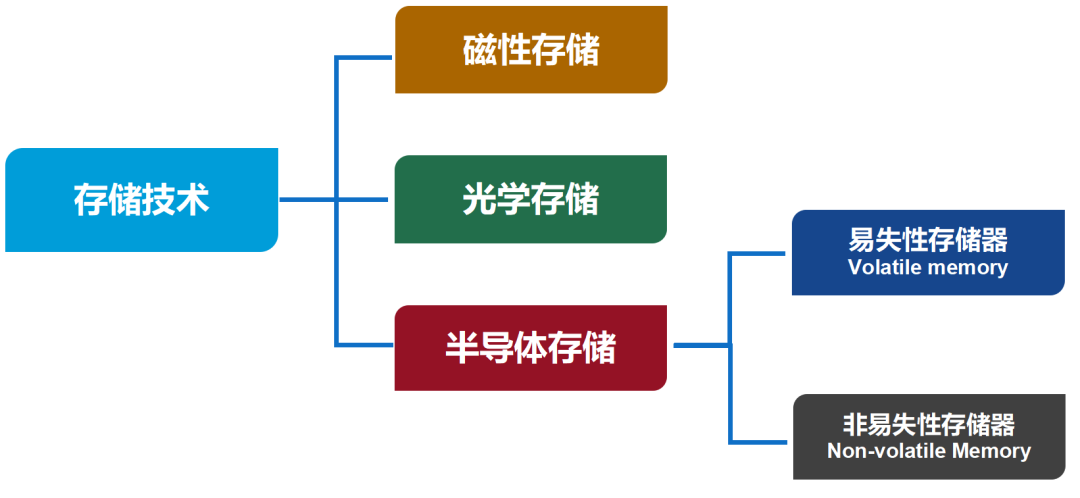
As the name implies, volatile memory cannot retain data after power is lost, while non-volatile memory can.
This is actually quite easy to understand. Those who have studied basic computer knowledge should remember that storage is divided into memory and external storage.
Memory, previously called operational memory, works in conjunction with the CPU when the computer is powered on. Once the power is off, the data is lost, which is classified as volatile (VM) memory.
On the other hand, external storage, which refers to hard drives, stores a large number of data files. When the computer is turned off, as long as you perform a save (write) operation, the data will remain, classifying it as non-volatile (NVM) memory.
Please note: Many resources now also classify semiconductor memory into Random Access Memory (RAM) and Read-Only Memory (ROM), which should sound familiar to everyone, right?
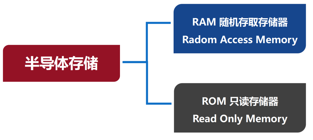
ROM (Read-Only Memory): It is easy to understand; it can be read but not written to.
RAM (Random Access Memory): Refers to its ability to “randomly read or write data from any storage unit in memory”, which is in contrast to traditional magnetic storage that must be “sequentially accessed”.
Some people think that volatile memory is just RAM, and non-volatile memory is just ROM. In fact, this is not precise.
Volatile Memory (VM)
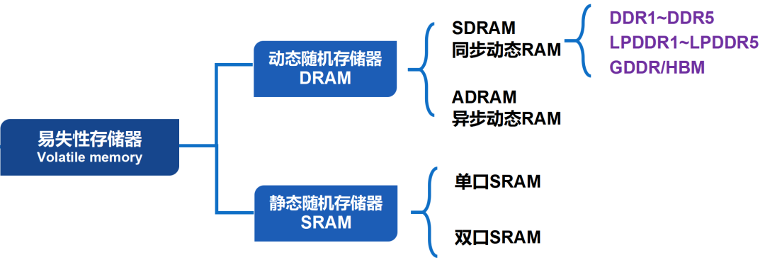
In the past few decades, volatile memory has not changed significantly and is mainly divided into DRAM (Dynamic Random Access Memory) and SRAM (Static Random Access Memory).
DRAM
DRAM consists of many repeating bit cells, with each basic unit composed of a capacitor and a transistor (also known as a 1T1C structure). The amount of charge stored in the capacitor is used to represent “0” and “1”. The transistor is used to control the charging and discharging of the capacitor.
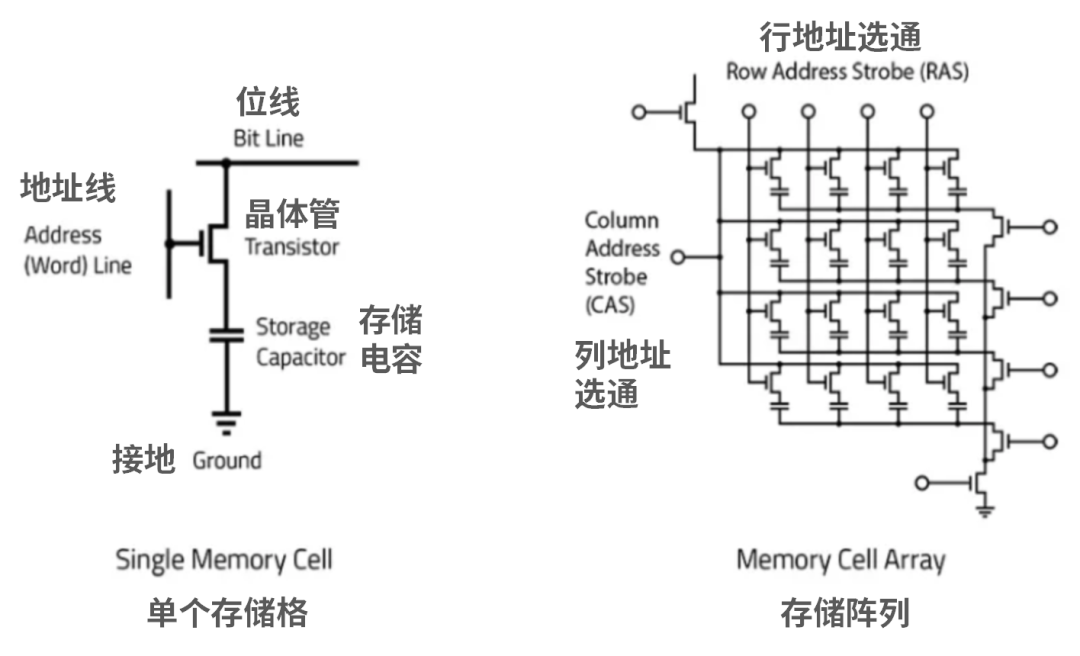
Because capacitors can leak, data must be periodically “dynamically” charged before changes or power loss to maintain the potential. Otherwise, data will be lost.
Therefore, DRAM is referred to as “dynamic” random memory.
DRAM has always been the mainstream solution for computer and mobile memory. Computer memory sticks (DDR), graphics card memory (GDDR), and mobile operational memory (LPDDR) are all types of DRAM. (DDR generally refers to DDR SDRAM, Double Data Rate Synchronous Dynamic Random Access Memory.)
It is worth mentioning that for graphics memory, besides GDDR, there is also a new type of memory called HBM (High Bandwidth Memory). It is created by stacking many DDR chips and packaging them together with the GPU (the memory chips are not visible externally).
SRAM
SRAM may be less familiar to everyone. In fact, it is the technology used for CPU cache.
The architecture of SRAM is much more complex than that of DRAM.
The basic unit of SRAM consists of at least 6 transistors: 4 MOSFETs (M1, M2, M3, M4) form two cross-coupled inverters, and 2 MOSFETs (M5, M6) are used to control the bit line switches, forming a latch (flip-flop) that locks binary 0s and 1s when powered on.
Thus, SRAM is referred to as “static” random memory.
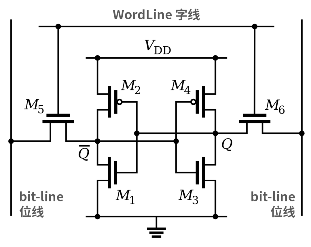
SRAM does not require periodic refreshing, has a fast response speed, but consumes more power, has a lower integration level, and is more expensive.
Therefore, it is mainly used in the main cache and auxiliary cache of CPUs. It is also used in FPGAs. Its market share has always been relatively low, making it less noticeable.
Non-Volatile Memory (NVM)
Next, let’s take a look at non-volatile memory products.
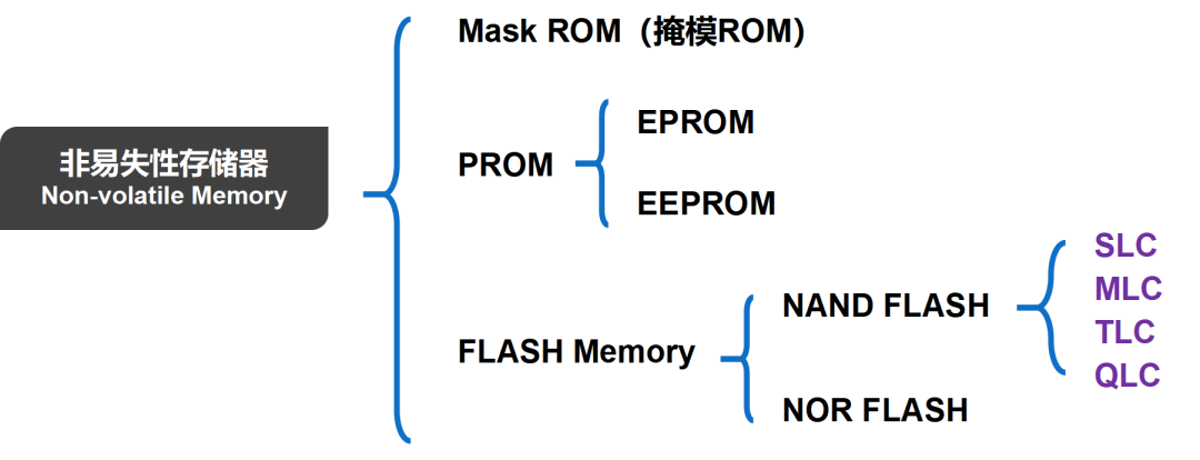
There are many technical routes for non-volatile memory products. The earliest was the aforementioned ROM.
The oldest type of ROM is the “true” ROM—completely read-only, with the content written at the factory and unable to be modified.
This type of ROM has very poor flexibility; if there is an error in the content, it cannot be corrected and must be discarded.
Mask ROM is a representative of this type of ROM. In simple terms, it directly uses a mask process to “engrave” information into the memory, making it unchangeable by the user, suitable for early mass production.
Later, experts invented PROM (Programmable ROM). This type of ROM can generally only be programmed once. At the factory, all memory cells are set to 1. Using specialized equipment, the fuses can be melted by current or light (ultraviolet) to achieve data rewriting.
PROM has greater flexibility than ROM, but still not enough. The best option is to modify the data, leading to the invention of EPROM (Erasable Programmable ROM).
The erasing method can be either light or electricity. The electric method is more convenient, and those that use electricity for erasing are called EEPROM (Electrically Erasable Programmable ROM).

EEPROM is modified at the byte level. This means it can write 0 or 1 to each bit, reading and writing by “bit” without needing to erase the entire content first. Its erase operation is also done on a “bit” basis, but the speed is still too slow.
In the 1980s, a technical expert from Toshiba, Fujio Masuoka, invented a brand new memory that could perform rapid erase operations—Flash memory.
Flash means “quickly” in English.
Due to space limitations, we will introduce the specific principles of FLASH next time. For now, we just need to know that Flash storage is erased in “blocks”.
The common block sizes are 128KB and 256KB. 1KB equals 1024 bits, which is several orders of magnitude faster than EEPROM that erases by bit.
Currently, the mainstream representative products of FLASH are only two: NOR Flash and NAND Flash.
NOR Flash
NOR Flash is a code-type flash memory chip, characterized by executing (XIP, Execute In Place) within the chip, meaning that applications do not need to read the code into the system RAM but can run directly in Flash memory.
Thus, NOR Flash is suitable for storing code and some data, with high reliability and fast reading speeds, offering performance and cost advantages in low to medium capacity applications.
However, the writing and erasing speeds of NOR Flash are very slow, and its size is twice that of NAND Flash, which limits its applications and results in a lower market share.
In the early days, NOR Flash was used in high-end mobile phones, but later, with the introduction of eMMC in smartphones, even this market was squeezed out.
In recent years, the application of NOR Flash has rebounded, with the market recovering. NOR Flash is now widely used in low-power Bluetooth modules, TWS earphones, mobile touch and fingerprint sensors, wearable devices, automotive electronics, and industrial control.
NAND Flash
In contrast, NAND Flash has a much larger market share.
NAND Flash is a data-type flash memory chip that can achieve large capacity storage.
It reads and writes data in pages and erases data in blocks, so although its writing and erasing speeds are about 3-4 orders of magnitude slower than DRAM, it is still 3 orders of magnitude faster than traditional mechanical hard drives, widely used in eMMC/EMCP, USB drives, SSDs, etc.
Earlier, eMMC was quite a hot topic.
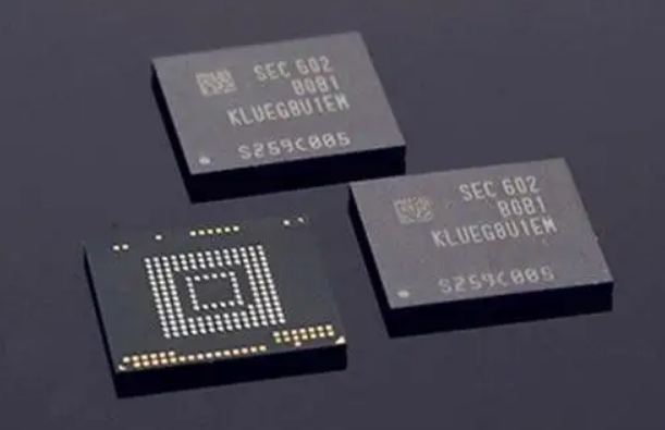
eMMC stands for embedded Multi Media Card, which packages the MMC (MultiMediaCard) interface, NAND, and the main controller into a small BGA chip, mainly to solve compatibility issues between NAND brands and facilitate manufacturers in quickly launching new products.
eMCP integrates eMMC with LPDDR to further reduce the module size and simplify circuit connection design.
In 2011, the UFS (Universal Flash Storage) 1.0 standard was born. Later, UFS gradually replaced eMMC, becoming the mainstream storage solution for smartphones. Of course, UFS is also based on NAND FLASH.
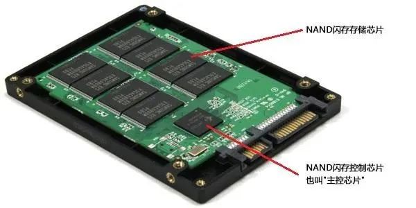
SSDs are quite familiar to everyone. They are basically all made using NAND chips and are currently developing very rapidly.
According to the differences in internal electronic unit density, NAND can be divided into SLC (Single-Level Cell), MLC (Multi-Level Cell), TLC (Triple-Level Cell), and QLC (Quad-Level Cell), representing the amount of data stored in each storage unit as 1 bit, 2 bits, 3 bits, and 4 bits, respectively.
From SLC to QLC, the storage density increases step by step, and the cost per bit decreases accordingly. However, performance, power consumption, reliability, and P/E cycles (erase/write cycle count, i.e., lifespan) will decrease.
In recent years, there has been significant debate in the DIY building community regarding SLC/MLC/TLC/QLC. Initially, netizens were concerned that the lifespan of SSDs would diminish. Later, they found that the reduction wasn’t as severe as expected, and the lifespan was still sufficient, so they gradually accepted it.
Early NAND was all 2D NAND. When the process technology entered 16nm, the costs of 2D NAND skyrocketed, and the difficulty and costs of planar miniaturization became unbearable. Thus, 3D NAND emerged.
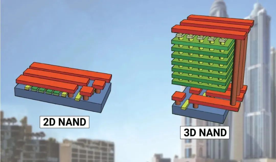
In simple terms, it is like moving from a flat house to a multi-story building, utilizing three-dimensional stacking to increase storage capacity and reduce the pressure of 2D NAND processing.
In 2012, Samsung launched the first generation of 3D NAND flash memory chips. Since then, 3D NAND technology has continued to develop, with increasing stacking layers and larger capacities.
New Types of Non-Volatile Memory
In 2021, IBM proposed the concept of “Storage-Class Memory” (SCM). IBM believes that SCM can replace traditional hard drives and serve as a complement to DRAM.
The exploration of new types of memory (media) is behind SCM.
According to industry consensus, new types of memory can combine the high-speed access of DRAM with the data retention characteristics of NAND flash after power is off, breaking the boundaries between memory and flash, merging them into one, achieving lower power consumption, longer lifespan, and faster speeds.
Currently, several types of new memory are prominent: Phase Change Memory (PCM), Resistive Memory (ReRAM/RRAM), Ferroelectric Memory (FeRAM/FRAM), Magnetic Memory (MRAM, with the second generation being STT-RAM), and Carbon Nanotube Memory.
Conclusion
Let’s revisit the classification diagram of semiconductor storage:
Focus on DRAM, NAND Flash, and NOR Flash, as these three types of memory account for over 96% of the market share today.
In fact, all memory types will find their place in the market based on their characteristics and provide their value.
Generally, the stronger the performance of the memory, the more expensive it will be and the closer it will be to computing chips (CPU/GPU, etc.). Weaker performance memories can meet demands with lower storage latency and insensitivity to write speeds, thus reducing costs.
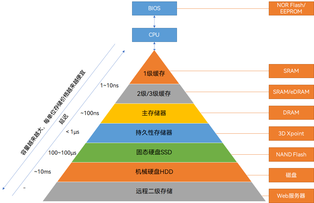
The evolution of semiconductor storage technology has always benefited from Moore’s Law, continuously improving performance while reducing costs. In the future, as Moore’s Law gradually loses effectiveness, where will semiconductor storage technology head, and can new types of storage media rise? Let’s wait and see.
Recommended Reading
-
Talent Development:
Huawei’s Major Product | Huawei Elite Learning Project
-
Content Series:
Huawei SUPER TALK | Talking About Voice
-
Technology Highlights:
Edge Computing | 5GtoB | Cloud-Edge Collaboration | Satellite Communication
Metaverse | 6G | Wi-Fi6 | 5G R17 | Solid-State Drives
-
Management Secrets:
The Booster of Innovation Capability | Second Track for Operators
How to Win the Gigabit Network Market | Six Elements for Strategic Implementation
-
Brand Stories:
New A Training Alumni Story Meeting | Hangzhou Training Center | Gui’an Training Center
More Exciting Videos
All atHuawei Training Video Channel
Give a “Like + Save + Follow” triple click below 👇