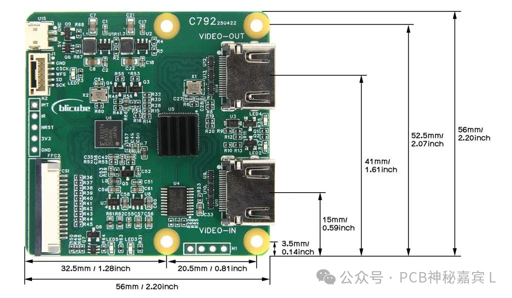
 PCB (Printed Circuit Board) is the core foundational component of electronic devices, often referred to as the “mother of electronic products.” It forms circuit connections on a common substrate according to a predetermined design, providing mechanical support, electrical interconnection, and signal transmission functions for electronic components. PCBs are widely used in almost all electronic products, including smartphones, computers, smart cars, communication base stations, and AI servers. The production process includes steps such as material cutting, inner layer fabrication, lamination, drilling, copper plating, circuit etching, solder mask application, and tin spraying. Modern high-end PCBs also involve advanced technologies such as High-Density Interconnect (HDI) and Flexible Printed Circuits (FPC).
01
Core Fundamental Concepts
(20 Items)
Essential starting points that determine the baseline of industry knowledge
- PCB Definition Printed Circuit Board, the supporting body and electrical connection carrier for electronic components.
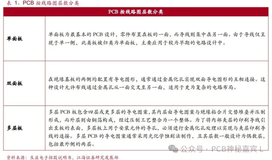
- Layer Classification Single-sided, double-sided, multi-layer boards (e.g., 4/6/8 layers).
- Substrate Insulating materials (e.g., FR-4 epoxy resin) that carry conductive traces.
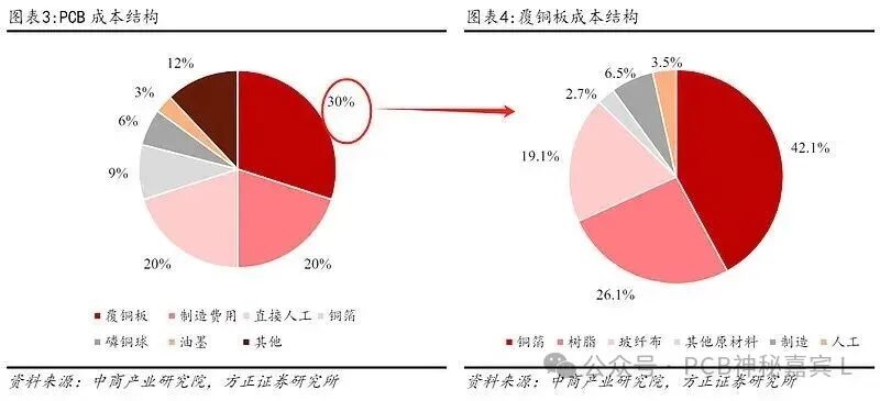
- Copper Clad Laminate (CCL) The core raw material for PCBs, composed of copper foil + resin + glass fiber cloth.
Copper Clad Laminate (CCL) is an abbreviation of three English words: Copper Clad Laminate. CCL is the core substrate for making printed circuit boards (PCBs), and its structure is formed by covering and laminating copper foil on the surface of an insulating substrate (such as resin, glass fiber cloth, etc.). This English name accurately reflects its material composition and process characteristics. Copper refers to the conductive material layer on the surface of the CCL. Clad means to cover or coat, describing the way the copper layer is bonded to the substrate. Laminate refers to laminated materials, emphasizing that CCL is made from multiple layers of materials (usually including substrate and copper foil) through a lamination process.
- Pad The metal area for soldering component pins.
- Via Drilled holes for electrical connections between layers, including through holes, blind holes, and buried holes.
- Trace Conductive copper lines that transmit signals or current.
- Silkscreen Text/symbol markings on the board surface to assist assembly.
- Solder Mask An insulating green oil layer that prevents short circuits.
- Gerber File The standard output file for PCB manufacturing, containing graphical data for each layer.
- DRC Check Design Rule Check, ensuring manufacturability.
- Netlist The electrical connection relationship between the schematic and the PCB.
- Footprint The definition of the pads and outline of components on the PCB.
- Placement The arrangement of component positions on the board.
- Routing The design of pathways connecting component pins.
- IPC Standards International standards for electronic industry processes and reliability (e.g., IPC-6012).
- SMT (Surface Mount Technology) The mainstream soldering process for components.
- THT (Through-Hole Technology) Traditional through-hole soldering process.
- Design for Manufacturability (DFM) Optimizing design to reduce production difficulty and cost.
- Thermal Management Heat dissipation solutions (e.g., heat holes, copper foil).
02
Fundamentals of Circuit Design
(20 Items)
Advanced skills that support the work of junior engineers
21.HDI (High-Density Interconnect): Micro-fine line/micro-hole technology used in miniaturized devices like smartphones.
HDI stands for High Density Interconnector or High Density Interconnection. The term “High Density” indicates high density, while “Interconnector” or “Interconnection” refers to interconnection, typically used to describe a high-density line connection technology in the field of printed circuit boards.
22.Impedance Control: Matching signal transmission impedance (e.g., 50Ω) to reduce reflections.23.Signal Integrity (SI): Ensuring signal transmission without distortion.24.Power Integrity (PI): Designing stable power supply systems.25.Electromagnetic Compatibility (EMC): Suppressing electromagnetic interference (EMI).26.Differential Pair Routing: Design for high-speed signals (e.g., USB, HDMI) to resist interference.27.Stack-up: The lamination order and material configuration of multi-layer boards.28.Copper Pour: Large area copper coverage to enhance shielding or heat dissipation.29.Teardrop: Reinforcement design at the connection between pads and traces.30.3W Rule: The principle of spacing between lines to avoid crosstalk.31.Design Software Tools: Altium Designer, Cadence Allegro, KiCad, etc.32.Panelization: Merging multiple PCBs for production to enhance efficiency.33.Test Point: Reserved access points for testing circuit functions.34.Stencil: Template for SMT solder paste printing.35.Reflow Soldering: Core process for SMT soldering.36.Wave Soldering: THT soldering process.37.ICT Testing: Online circuit function testing.38.Flying Probe Testing: PCB continuity testing without test fixtures.39.IPC-A-600: PCB appearance acceptance standards.40.IPC-7351: Packaging design specifications.
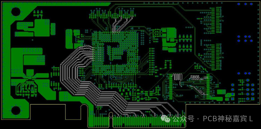
PCB Layout
03
Materials and Processes
(20 Items)
Key manufacturing factors that affect cost and performance
41.Tg Value: Glass transition temperature of the substrate, measuring heat resistance (e.g., Tg≥170℃).42.High-Frequency Materials: Rogers, PTFE, used for 5G/radar.43.Copper Foil Thickness: Commonly used 1oz (35μm), 2oz (70μm).44.ENIG (Electroless Nickel Immersion Gold): Surface treatment process with good oxidation resistance.45.HASL (Hot Air Solder Leveling): Low-cost surface treatment with lower flatness.46.OSP (Organic Solderability Preservative): Environmentally friendly surface treatment.47.Laser Drilling: Micro-hole processing technology for HDI boards (hole diameter ≤0.1mm).48.Plated Through Hole: Filling copper in micro-holes to enhance reliability.49.LDI (Laser Direct Imaging): High-precision graphic transfer technology.50.Etching: Removing excess copper foil to form traces.51.Lamination: The process of pressing multi-layer boards together.52.Solder Mask Opening: Exposing pad areas.53.V-Cut: Panel separation process.54.Warpage: PCB flatness indicator.55.CAF (Conductive Anodic Filament): Copper ion migration causing short circuits in humid environments.56.CTE (Coefficient of Thermal Expansion): Parameter for material deformation due to heat.57.TDR Testing: Impedance measurement method.58.AOI (Automated Optical Inspection): Automatic screening for circuit defects.59.X-Ray Inspection: Detection of internal structural defects.60.Ion Contamination Testing: Cleanliness verification.
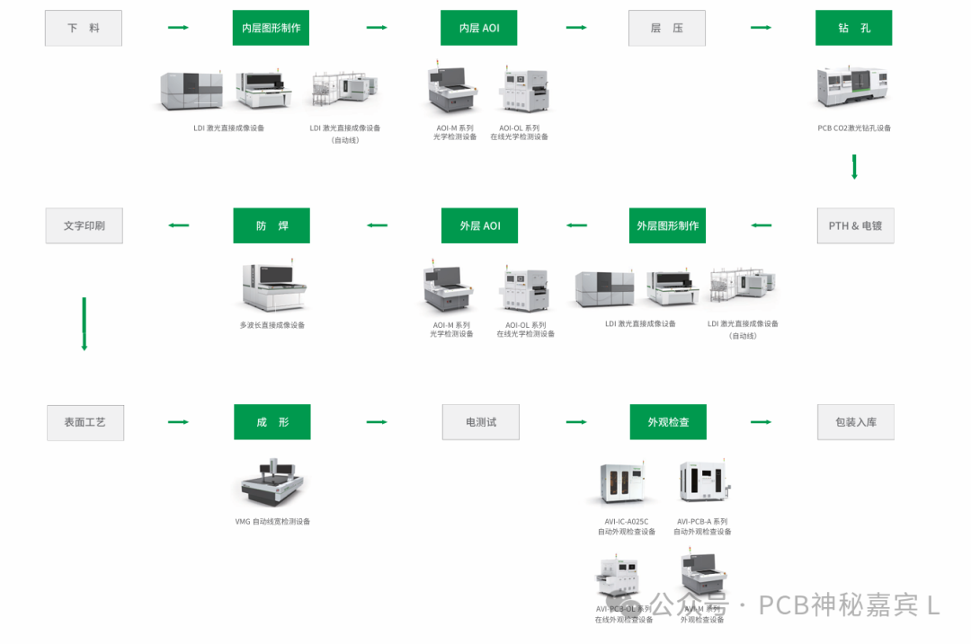 Introduction to PCB Processes
04
Advanced Technologies
(20 Items)
Core capabilities for intermediate engineers to solve complex problems
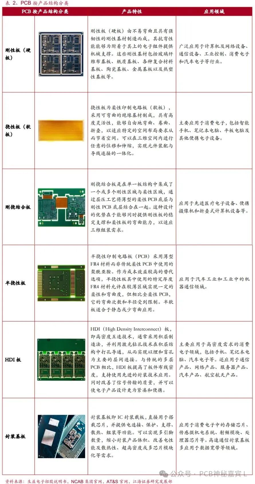
61.IC Substrate: PCB specifically for chip packaging (e.g., FC-BGA).62.Flexible Circuit Board (FPC): Bendable PCB used in mobile phones/wearable devices.63.Rigid-Flex Board: Composite design of rigid and flexible areas.64.Back Drilling: Removing excess copper pillars to reduce signal reflection.65.Embedded Resistors and Capacitors: Internal embedded resistors/capacitors to save surface space.66.Signal Termination: Matching end resistors to suppress reflections.67.Power Segmentation: Segmentation of plane layers for multiple voltage domains.68.Cross-Segmentation Design: Avoiding high-speed signals crossing plane segmentation.69.Serpentine Routing: Equal-length routing technology.70.π Filter: Circuit for suppressing power noise.71.Thermal Simulation: Software predicting PCB temperature rise.72.SI/PI Simulation Tools: HyperLynx, Sigrity, ADS.73.EMC Simulation: Predicting electromagnetic interference.74.DDR Routing Rules: High-speed design specifications for memory interfaces.75.PCIe Routing Rules: High-speed serial bus design specifications.76.RF Routing: Special design for high-frequency circuits (e.g., curved corners).77.Mixed Signal Design: Layout strategies for coexisting analog/digital circuits.78.Design Reuse (Reuse Block): Modular design to enhance efficiency.79.DFA (Design for Assembly): Optimizing assembly processes.80.DFT (Design for Testability): Facilitating later testing.
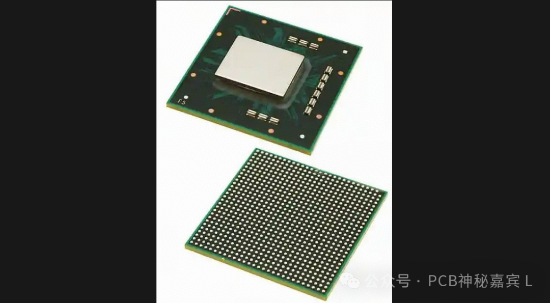
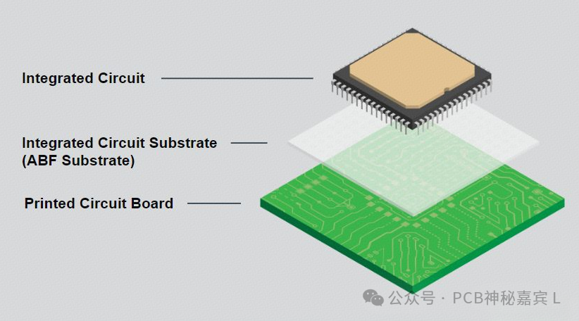 IC Substrate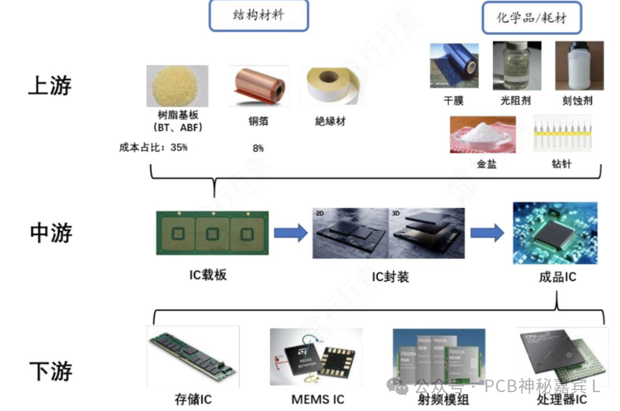
05
Industry Frontiers and Trends
(20 Items)
Senior engineer’s perspective to grasp technological directions
81.Cowos/Cowop Process: Chip packaging technology (Cowos requires ABF substrate, Cowop directly integrates PCB).82.ABF Material: Ajinomoto build-up film, core material for IC substrates.83.AI Server PCB: Layer counts reaching 20-30 layers, with prices 5-7 times that of traditional ones.84.Automotive PCB: Explosive demand for electric vehicle main control boards and radar boards.85.Low Loss Materials (Df/Dk): Reducing signal attenuation (e.g., ultra-low loss Megtron 6).86.mSAP Process: Semi-additive process for making ultra-fine lines (line width/spacing ≤40μm).87.RDL (Re-Distribution Layer): Advanced packaging interconnection technology.88.SiP (System in Package): Multi-chip integrated packaging.89.2.5D/3D Packaging: TSV silicon through-hole interconnection technology.90.Optical Module PCB: Demand for 800G/1.6T high-speed modules (e.g., low dielectric loss).91.High-Frequency High-Speed CCL: Shengyi Technology leading the market (30% market share).92.Domestic Substitution: Shenghong Technology (NVIDIA supplier), Huadian Co. (GB300 certified).93.Southeast Asia Capacity Layout: Addressing supply chain risks (e.g., Shenghong’s Vietnam base).94.Environmentally Friendly Materials: Halogen-free substrates, biodegradable PCBs.95.Mini LED PCB: Ultra-thin high thermal conductivity substrates.96.Quantum Computing PCB: Material adaptability for extremely low-temperature environments.97.AI Quality Inspection: Deep learning replacing AOI defect determination.98.Prismark Data: Authoritative industry report (global PCB output value of $78.6 billion in 2025).99.Supply-Demand Gap: Expected 17% gap in AI PCB by 2026.100.CAGR 8.3%: Growth rate of the HDI PCB market from 2025 to 2032.
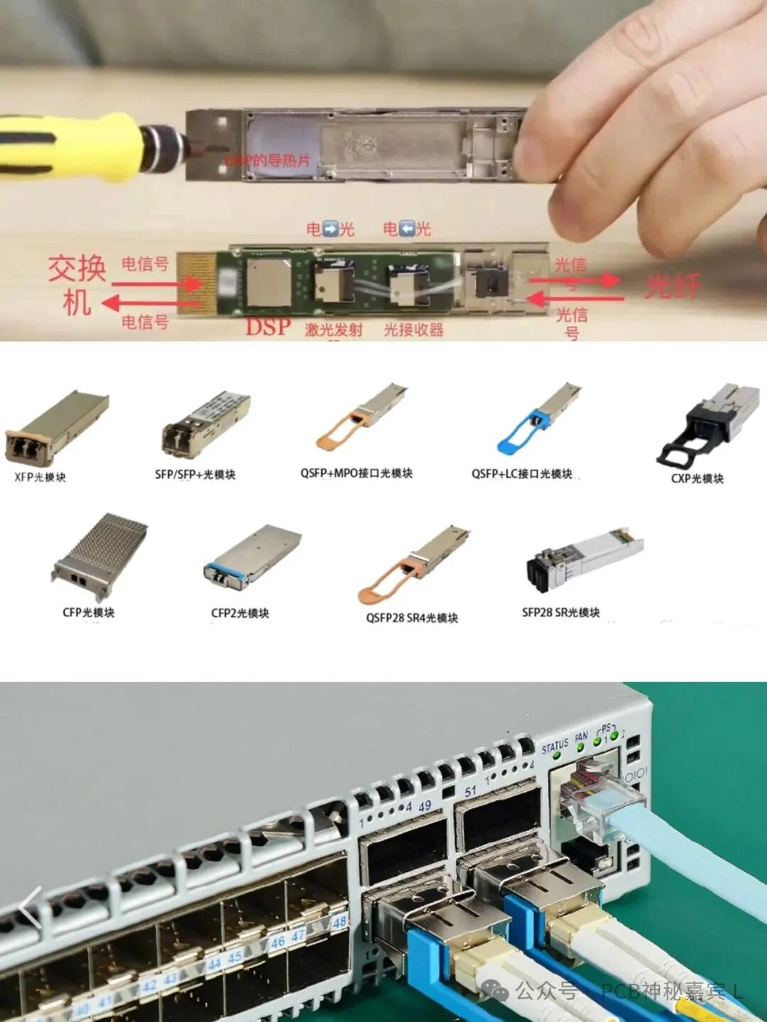 Optical Module
Currently, the explosive demand for AI computing power is driving a structural shortage of high-end PCBs:
1) Demand for technological upgrades: The layer count of AI server PCBs has increased from 14-24 layers in traditional servers to 20-30 layers, with a single unit value reaching 5-7 times that of traditional servers. Prismark data shows that the global PCB output value will reach $73.6 billion in 2024 (up 5.8% year-on-year), and is expected to increase to $78.6 billion in 2025, with AI servers and high-performance computing (HPC) contributing core increments.
2) The window for domestic substitution has opened: Domestic companies are breaking through high-end PCB technology barriers. For example, Shenghong Technology has mass-produced 70-layer high-precision circuit boards, supplying leading customers like NVIDIA and AMD; Huadian Co. has over 30% market share in the AI server PCB sector, with a gross margin of 35%-40%. Dongshan Precision will invest no more than $1 billion to build high-end PCB projects. This $1 billion investment is considered large-scale in the printed circuit board industry, especially among specialized PCB manufacturers. The expansion will promote the increase in the proportion of high-density interconnect (HDI) and rigid-flex boards, optimizing product structure.
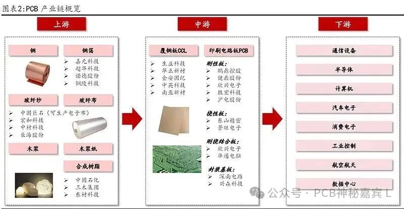
3) Synergistic effects in the industrial chain: High-end PCBs rely on upstream high-frequency high-speed copper clad laminates (CCL), special glass fiber cloth, and other materials. The price of CCL for AI use is 2-2.5 times higher than traditional products, but the monopoly situation of Japanese companies is being broken— Shengyi Technology has increased its market share of high-frequency high-speed CCL to 30%, providing domestic material companies with incremental opportunities.
Looking ahead, the resonance of AI inference chip iteration, automotive computing power upgrades, and the consumer electronics replacement wave is expected to extend PCB order visibility until 2027; with the explosive demand for inference, ASIC servers and high-speed switches are expected to experience rapid growth, and the supply-demand gap for computing power PCBs is expected to widen. Institutions estimate that the global AI PCB supply-demand gap will still reach 17% by 2026. Expansion will reshape the industry landscape, with rapid increases in capacity for high-layer boards, HDI, and flexible boards, and the high-end PCB market scale is expected to grow faster. Attention should be paid to leading PCB companies with high-end capacity layouts and related upstream companies such as copper foil and ABF substrates.
Source: https://stock.jrj.com.cn/2025/07/29074852036358.shtml#rss
end

Image: Source from the internet
Editor: Mysterious Guest L