Signal Isolation
Once we have resolved the design and control issues of the switch structure, the next question is to determine the isolation strategy.
Each interface in the power gating area needs to be managed. We need to ensure that turning off the power in this area does not cause short-circuit currents at the inputs of any power modules. We also need to ensure that the floating outputs of the power-down block do not cause false behavior in the power-up block.
The outputs of the power gating blocks are the primary concern, as they can lead to electrical or functional issues in other blocks. The inputs of the power gating modules are usually not a problem—they can be driven to valid logic levels by the power-up modules without causing electrical (or functional) issues in the power-down modules.
Signal Isolation Techniques
The basic method for controlling the output of the power-down module is to use isolation units to clamp the output to a specific, valid value.
There are three basic types of isolation units: those that clamp the signal to “0”, those that clamp the signal to “1”, and those that clamp the signal to the most recent output value.
In most cases, clamping the output to an inactive state is sufficient. When using active-high logic, the most common method is to clamp the value to “0”, which is achieved with AND gate functionality. When using active-low logic, OR gate logic will hold the output at logic “1”.
As long as the control input is in the appropriate “isolation” state, the design of the clamp library units can prevent floating input signals from causing short-circuit currents and leakage paths. Additionally, their synthesis models typically have extra attributes to ensure that these units are never optimized, buffered incorrectly, or inverted as part of logic optimization.
Figure 5-2 on the left shows a conceptual view of the clamping with an AND gate. When the isolation signal “ISOLN” is high, the signal passes to the output; when “ISOLN” is low, the output is low:
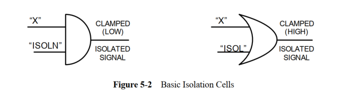
The right side of Figure 5-2 shows the conceptual view of clamping with an OR gate structure. When the isolation control signal “ISOL” is high, the output is clamped high;
These clamping gates introduce delays to the isolated signals. For certain critical paths, this added delay may be unacceptable—such as in high-speed cache memory interfaces.
Another isolation technique that does not introduce delay is to use pull-up or pull-down transistors. However, this method introduces multiple drivers in the power gating network, requiring careful ordering to avoid signal contention. Even if the pull-up or pull-down transistors are relatively weak devices, when the total number may be large enough, excess current from bus contention can cause issues. The ordering behavior to avoid contention is handled by the power controller.
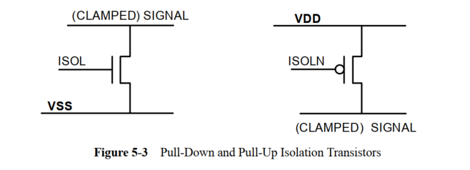
Figure 5-3 on the left shows a conceptual view of pull-down clamping; when “ISOL” is high, the output is pulled low.
Figure 5-3 on the right shows a conceptual view of pull-up clamping; when “ISOLN” is high, the signal passes to the output.
To avoid output glitches, it is important to keep the output stable during power-up until the power is stable. This behavior is straightforward for clamp units, but quite challenging for pull-up/pull-down transistors, as their output values may conflict when they are recovering power, potentially causing changes in output values.
Note that transistor-based clamping can lead to metal migration and reliability issues, even with small continuous currents flowing through them. They also pose a significant testing challenge—any time multiple drivers are present, testability becomes very difficult.
Therefore, although pull-up and pull-down transistors have lower area and timing costs, they are not recommended for RTL design. Instead, it is advisable to use gate-level style circuits, which will be described in the remainder of this section. However, the pull transistor method can be quite useful in special cases, such as when there are timing-critical paths.
Output or Input Isolation
As mentioned above, to avoid floating output signals driving the inputs of the power-up module and causing electrical issues, it is necessary to isolate the outputs of the power gating module. Logically, it does not matter whether we handle these signals at their source (i.e., within the power gating module) or at their destination (i.e., within the power-up module).
However, there are some important practical considerations that affect this choice.
It is quite likely that some outputs of the power gating block are connected to more than one power-up block. If the outputs are isolated at the receiving block, each output may require multiple isolation units. Therefore, isolating the outputs within the power gating block can improve area utilization and reduce area.
Isolating outputs within the power gating block also makes analysis easier. Once we determine that all outputs are correctly isolated, we have completed the check. If these signals are isolated in the receiving block, we must check each fan-out of the output signals to ensure that there is at least one isolation unit on each. When reusing this design in different designs, this analysis must be performed again in each case.
However, setting isolation at the source does impose some constraints on placement and routing. Unlike other gates in the power gating group, isolation units must remain powered during power-down. Therefore, the power domain containing the power gating block must provide both switched power and always-on power domains. This somewhat complicates the power routing of the chip, but modern EDA tools can handle this issue.
Regardless of whether the output is isolated at its source or destination, EDA tools must maintain the uniqueness of the isolation units. If the isolation is at the source, the tools cannot use buffers in the power gating to buffer the output of the isolation unit, as that buffer is not in the always-on domain. If the isolation unit is at the destination, the tools cannot buffer (pre-isolated) signals with buffers from the always-on domain. The control signals sent to the isolation unit must be buffered through always-on domain units.
Additionally, optimizations during placement and routing cannot replace isolation units with non-isolation units.
For the reasons mentioned above, we strongly recommend using designs with isolation units in reusable IP to hide the complexity of isolation in SoC-level integration.
Interface Protocols and Isolation
When designing the interfaces of power gating blocks, there are two goals: to minimize leakage and to avoid unnecessary or erroneous behavior.
Consider a case where the output of a power gating block points to an always-on block. When the power gating module is powered down, the power module receives clamped signal values. If these signals are active-high and at a high level, the destination may interpret these signals as commands and behave incorrectly. Clamping the signals to an inactive state is the best strategy to avoid this issue. For most designs, this means clamping the output to “0”.
One possible exception to this guideline is reset. Typically, reset is active-low, so clamping low signals shows a reset state on the interface. In fact, this may be the most appropriate driving reset value when the power is off. This ensures that the reset will be effective during power-up. In any case, it is necessary to consider whether the clamped interface signals are valid or invalid when powered down.
Now consider a case where a power gating block has outputs to another (independent) power gating block. Since the blocks are independent power gating units, their outputs must be isolated. However, in some cases, the source block will be powered down, and the target block will also be powered down. In this case, if the clamped signal is at the wrong level, it may lead to increased leakage currents. For example, if switching VDD (for the target block), the output (source block) is clamped to “1”, there may be a current path from the clamped output to ground. This could cause unnecessary leakage.
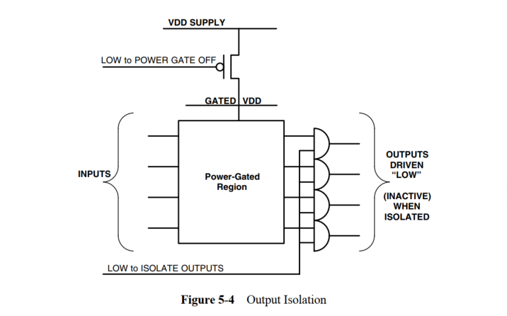
Therefore, for header switch designs, the recommendation is to use active-high signals and active-low resets, and clamp all signals to “0”.
For complex protocols, it may be necessary to use more sophisticated isolation strategies: clamping signals to their last value. This method allows the protocol to restart in the process rather than starting in the reset state. This strategy requires a latched isolation unit, which may not be available in all libraries, so it should only be used when absolutely necessary.
Recommendations and Pitfalls in Isolation Techniques
Recommendations:
Isolate the outputs of the power gating module.
Use isolation units instead of pull-up or pull-down clamping, unless using very specialized interface protocols (in which case, the complexity challenges of “multiple drivers” may be worth implementing).
Ensure that stuck-at-0 and stuck-at-1 faults can be detected when testing isolation control signals. This helps verify that isolation is effective during manufacturing testing.
Pitfalls:
Ensure that isolation units are always powered.
Due to clock tree synthesis and timing convergence, isolation clamping on clocks is quite complex. Balancing the clock tree is particularly difficult. If possible, avoid generating clocks in the power gating block and using external blocks.