
What type of sample do you have in your hands?If it has not undergone Corner verification and reliability testing, you need to pay more attention~ This is also why many companies prefer to choose mass-produced chips that have been verified by leading enterprises;
Today, I will introduce to you the key steps that generally take place after chip design is completed.
Table of Contents:
-
What is MPW? Why MPW?
-
Understanding MPW from the Perspective of Wafer Production
-
What is FullMask?
-
What is ECO?
-
What is a Corner Wafer?
1
What is MPW? Why MPW?
Wafer fabs have a fixed number of MPW opportunities each year, called Shuttle, which departs on schedule, isn’t that very vivid?
When different companies share a wafer, there must be rules; MPW locks the area by SEAT, with one SEAT generally being a 3mm*4mm area. Typically, wafer fabs will limit the number of SEATs reserved for each company to ensure participation in MPW by different chip companies; (Actually, if there are too many SEATs, the cost will go up, and the significance of MPW will diminish.)
Since it is a shared wafer, the number of chips obtained through MPW will be very limited, mainly used for internal verification testing by chip companies, and may also be provided to a very small number of leading customers;
From this, you may have understood that MPW is an incomplete, non-mass-producible wafer;
So, why do MPW?
Because chip investment is too expensive, and for new processes or significantly changed new designs, if there are design issues, the worst result of wafer production may be that it cannot light up, or critical functions and performance do not meet expectations, resulting in losses ranging from hundreds of thousands to tens of millions;
The cost of MPW is small, generally only a few hundred thousand, which can greatly reduce risks;
It should be noted that since MPW is a complete production process from the production perspective, it still takes time; one MPW generally requires 6 to 9 months, which will delay the delivery time of the chips;
2
Understanding MPW from the Perspective of Wafer Production
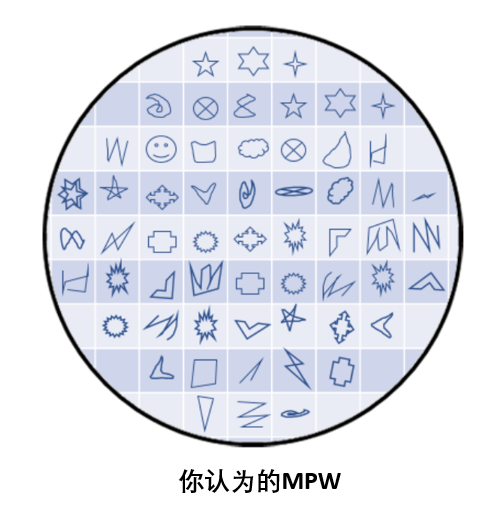 Image: CUMEC Service Platform
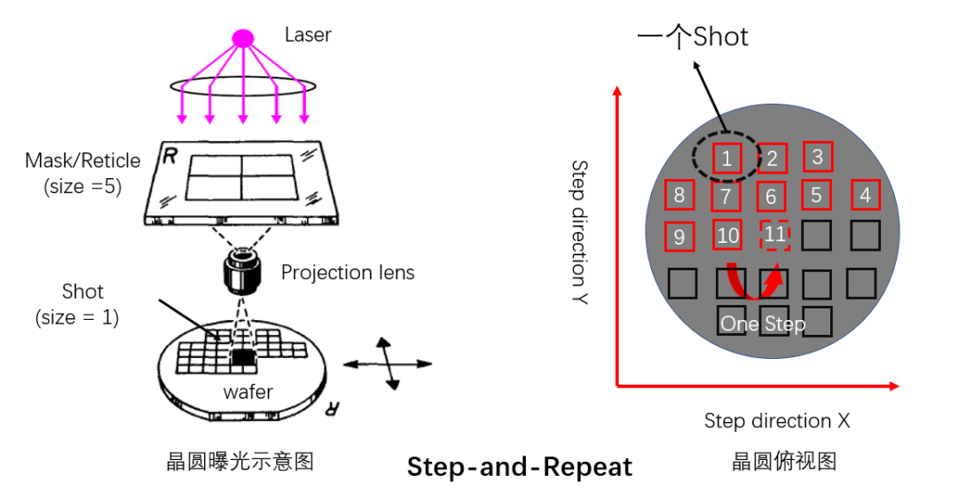 Image: CUMEC Service Platform
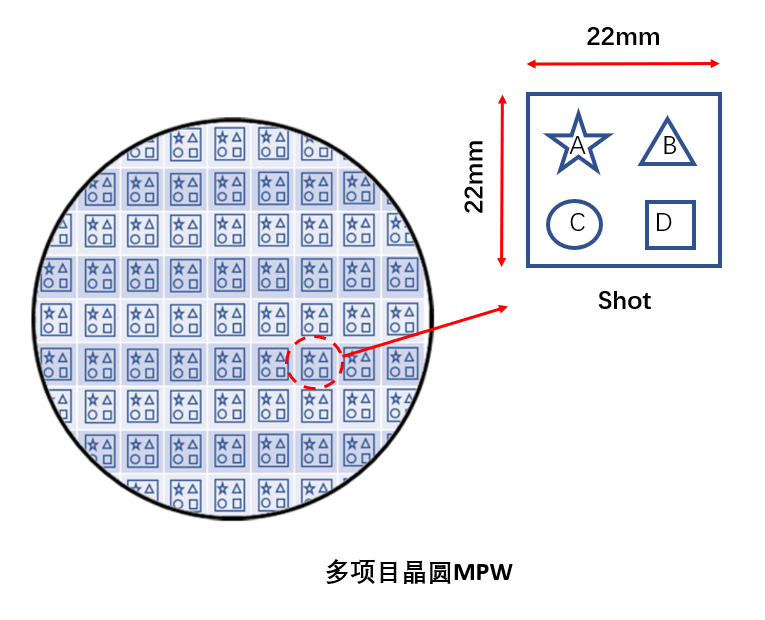 Image: CUMEC Service Platform
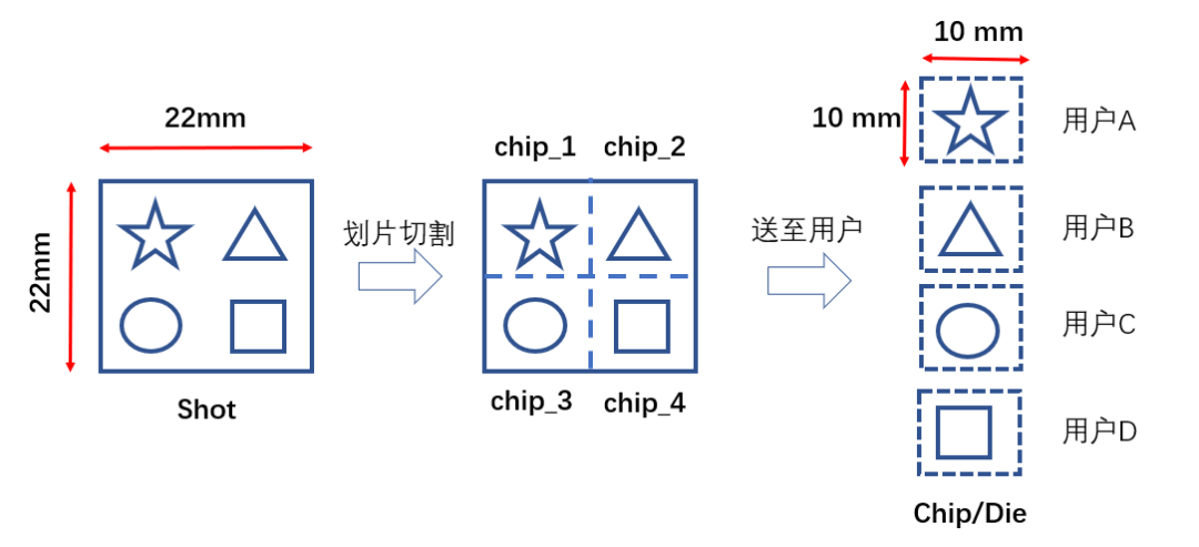 Image: CUMEC Service Platform
Generally, MPW wafers can share a maximum of 20 users;
3
What is FullMask?
FullMask, meaning “full mask,” indicates that all masks in the manufacturing process serve a specific design, meaning that all shots in the previous section belong to the same company;
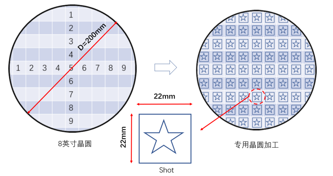 Image: CUMEC Service Platform
Chips using FullMask can produce thousands of dies from one wafer; then packaged into chips, they can support large-scale customer demand;
4
What is ECO?
If the chips from MPW or FullMask have functional or performance defects, a revision is needed, and the term ECO is often used;
ECO can occur before, during, or after Tapeout; ECO after Tapeout may require minor changes to a few Metal layers, while significant changes may involve altering dozens of Metal layers or even re-taping;
Some chip design companies can perform ECO more than five times, which has refreshed my understanding;
5
What is a Corner Wafer?
As we know, the manufacturing of chips is a chemical & physical process,
process deviations (including doping concentration, diffusion depth, etching degree, etc.) can lead to performance differences between different batches of wafers, between wafers of the same batch, and between different chips on the same wafer.
On one wafer, it is impossible for the carrier drift velocity at every point to be the same; as voltage and temperature vary, their characteristics also differ, categorizing them leads to PVT (Process, Voltage, Temperature).
Process can be further divided into different corners:
-
TT: Typical N Typical P
-
FF: Fast N Fast P
-
SS: Slow N Slow P
-
FS: Fast N Slow P
-
SF: Slow N Fast P
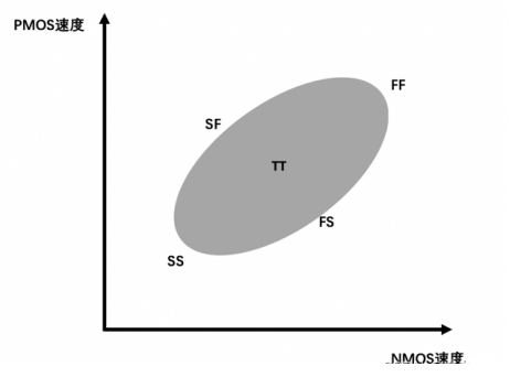
To ensure performance, before formal mass production, chips will be specifically tested with Corner wafers to verify that process deviations are within design limits;
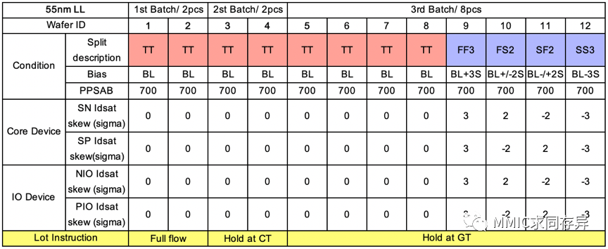
Below is an example of a 55nm Logic process wafer, with the proposed corner split table.
Reprinted from MMIC, seeking common ground while reserving differences.
-
#1 & #2 Two pilot wafers, one blind-sealed, one measuring CP
-
#3 & #4 Two wafers held in Contact, reserved for later revisions, which can save ECO tape time
-
#5~#12 Eight wafers held in Poly, waiting for pilot results to see if adjustments are needed for device speed, and to verify corners
-
In addition to leaving enough chips for testing and verification, Metal Fix, it is also necessary to reserve as many wafers as possible for mass production shipment based on project needs.
MMIC Seeking Common Ground While Reserving Differences: Introduction to Corner Wafer