In the debugging of JESD204C on the board, I directly skipped the process of looking at its examples, as the content of the example block design is quite extensive and seems cumbersome. Since I already have experience debugging JESD204B, I simply followed the same approach for JESD204C, connecting some key lines to create a top-level module with both transmission and reception, and then simulating through a loopback.
Clearly, as an ADC and DAC interface, we need to construct a top-level module.
1. IQ input, as the data source for the DAC.
2. IQ output, as the data collected by the ADC.
3. AXI bus, used for configuring the IP core.
4. Several reset lines, used to reset the PHY and AXI.
5. Clock.
6. Interface with external JESD devices on the FPGA (high-speed interface pins/SYSREF/reference clock).
JESD204B: 4T4R 4-lane sampling rate 245.76 Mbps, 9.8304 Gbps rate.
JESD204C: 4T4R 4-lane sampling rate 245.76 Mbps, 8.11008 Gbps rate.
Using JESD204C, the SERDES can operate at a lower rate to achieve the same data volume as JESD204B.
The difference is that JESD204C uses 64B/66B encoding, with an IP core output data width of 64 bits per lane, and a corresponding clock of 122.88 MHz. In contrast, JESD204B uses 8B/10B encoding, with an IP core output data width of 32 bits per lane, and a clock of 245.76 MHz. Therefore, the IQ mapping and demapping module in JESD204C applications also requires a clock domain conversion.
The specific implementation block diagram is as follows:
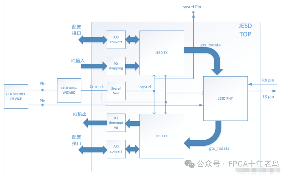
AXI conversion: The JESD CORE uses the AXI interface. Unless directly connected to the ZYNQ SOC, protocol conversion is necessary for proper operation.
IQ MAPPING/DEMAPPING: The arrangement of IQ data settings is related to the chip settings, which may require configuring IQ high/low bits, endianness, etc., as well as cross-clock domain conversion.
SYSREF GEN: This module is used to generate SYSREF, which is provided to the JESD CORE and external JESD chips. It can be generated internally using CORECLK. This SYSREF can also be input through external pins.
Several signals to pay attention to during debugging:
1. gtx_rxblock_sync should be 1, and rx_tvalid should also be 1. If both are 1, the FPGA side is receiving correctly. At the same time, the external chip should also check if it is receiving synchronization and functioning normally, and verify the link establishment flag on both sides to confirm that there are no issues.
2. Loopback: The JESD PHY has a gtx_loopback_in port used for configuring RXTX high-speed interface loopback, which is useful when there are issues during board debugging. It is also used initially to check if the link can be established and if the data is normal.
3. Pre-emphasis parameters:
.gtx_txpostcursor_in
.gtx_txprecursor_in
.gtx_txdiffctrl_in
When signal quality is judged to be poor, these parameters can be adjusted. Before adjusting these parameters, establish an IBERT eye diagram for scanning.
4. Operational process (this is an additional step compared to the JESD204B IP core, important):
At least the 0x24 register of the transceiver core needs to be operated on.
Writing 2 to the 0x24 register indicates the start of the data channel. This must be written; otherwise, transmission will not begin. The command channel can remain off, and the data channel can operate independently.
The 0th bit is for the command channel, and the 1st bit is for the data channel. The 0th bit is related to command and data verification.The 1st bit of the data channel, if 0, sends a scrambled 0; if 1, sends and receives normal data. This register is very important; the data channel bit must be set to 1; otherwise, normal data will not be received. If the command channel is used, the command channel bit must also be set to 1.
If this article has been helpful to you, please remember tofollowour public account, which will continue to update topics related to FPGA technology. Thank you!
Unauthorized reproduction and copying are prohibited without the author’s permission!