Introduction: UART is a universal serial data bus used for asynchronous communication. This bus supports bidirectional communication, enabling full-duplex transmission and reception. UART is commonly used for data communication with PCs, as well as for the transmission of command and control information. In this article, we will introduce the UART communication protocol, transmission timing, and how to implement FPGA communication with a PC using HDL programming.
1. Understanding Asynchronous Serial Communication
First, we need to introduce a few concepts.
Communication Protocol: Refers to the rules and agreements that both parties must follow to complete communication or service. What to communicate, how to communicate, and when to communicate must adhere to mutually acceptable rules. These rules constitute the communication protocol.
Serial Communication: Refers to a communication method where both parties communicate bit by bit, following a specific timing sequence. In serial communication, data is transmitted bit by bit, with each bit occupying a fixed time length, allowing information exchange between systems using only a few communication lines, making it particularly suitable for long-distance communication between computers and peripherals.
Asynchronous Communication: This is in contrast to synchronous communication. In asynchronous communication, the time slots between the characters being sent can be arbitrary. Of course, the receiving end must always be ready to receive (if the power of the receiving host is not turned on, then sending characters from the sender is meaningless, as the receiver cannot receive them at all). The sender can start sending characters at any time, so it must add markers at the beginning and end of each character, namely start bits and stop bits, to ensure that the receiver can correctly receive each character.
2. Introduction to UART Communication Protocol
UART uses an asynchronous serial communication mechanism, and its data transmission protocol format is shown in the figure below.
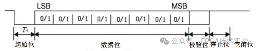 Figure 1: UART Data Transmission Protocol FormatThe meanings of each bit are as follows:Start Bit: A logical “0” signal is sent first, indicating the start of character transmission.Data Bits: Can be 5 to 8 bits of logical “0” or “1”. For example, ASCII code (7 bits), extended BCD code (8 bits).Parity Bit: After adding this bit to the data bits, the number of “1” bits should be even (even parity) or odd (odd parity); the parity bit for the data can be optional; if parity is not used, then this bit does not exist.Stop Bit: It is an end marker for a data field. It can be 1 bit, 1.5 bits, or 2 bits of high level.
Idle Bit: In a logical “1” state, indicating that there is currently no data information being transmitted on the line.
The UART data transmission protocol format usually needs to be predefined by the transmitting and receiving devices, such as the number of data bits to be transmitted, whether a parity bit is needed, and the stop bit. Another important parameter is the baud rate of data transmission.
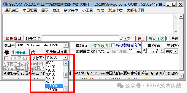
Figure 2: Common Standard Baud Rates
The speed of UART data transmission is usually measured in baud rate. During a serial communication process, the data receiving and sending parties do not share a clock, so both sides must agree on the baud rate for data transmission. Based on the agreed transmission rate, the time interval between adjacent bits will be fixed, allowing the receiving end to sample the data from the sending end.
Standard baud rates include 2400bps, 4800bps, 9600bps, 19200bps, 38400bps, 57600bps, 115200bps, etc. Of course, higher speeds mean higher sampling requirements, which may gradually increase the error rate. 3. Data Transmission Workflow
In this article, we set the transmission protocol as: 1 start bit + 8 data bits + 1 stop bit, with no parity bit, and a transmission baud rate of 9600bps.
(1) The sender sends according to the pre-defined transmission protocol and baud rate:
1 bit start bit + 8 bit data bits + 1 bit stop bit
Where the start bit is logical 0 (low level), the stop bit is logical 1 (high level), and the sender is in idle state at 1.
(2) Receiver: The receiver determines the start of a data packet by detecting the transition from level “1” (idle state) to “0” (start bit). After confirming the start bit is received, it sequentially receives data using a higher sampling clock to complete data acquisition. After receiving the data bits, it continues to receive the stop bit.
4. Hardware Introduction
The hardware uses a USB to RS232 chip CP2104 to achieve communication between the PC and FPGA. The circuit is designed with an ESD protection chip RCLAMP0522P, which, together with the conversion chip CP2104, can prevent static surges from damaging the FPGA chip, providing isolation and protection.
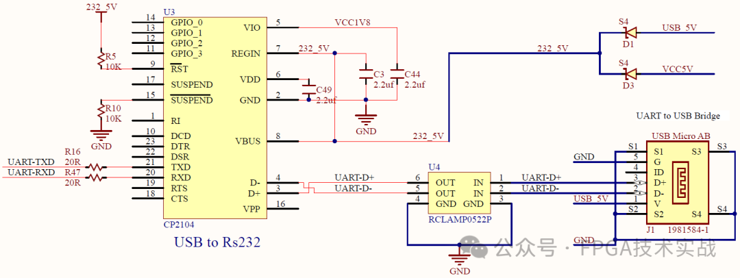 Figure 3: USB to RS232 Circuit Diagram5. Software Design
The software design is divided into two modules: uart_rx.v for receiving and uart_tx.v for transmitting, with the top-level module uart_driver.v interconnecting the two modules, as shown in the figure below.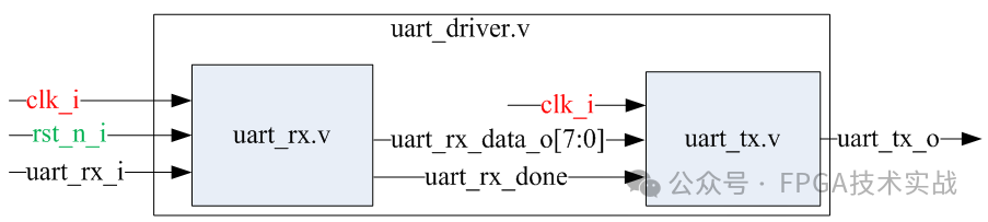
Figure 4: Software Module Division
UART data transmission mainly includes two parts:
- Design of baud rate generation;
-
Data transmission design, including receiving and sending.
(1) Baud Rate Generation Design:The onboard FPGA input clock is 100MHz. To obtain common baud rates, a counting division method is used. BAUD_DIV=100000000/baud rate. The sampling center point is the midpoint of the sending or receiving clock, i.e., BAUD_DIV_CAP=100000000/(2*baud rate).(2) Data Transmission DesignData receiving module: Under the set transmission baud rate of 9600bps, according to the serial transmission timing, perform deserialization (serial to parallel conversion). In idle state, the received data is a logical high level, waiting for the arrival of the start bit logical low level. When the start bit arrives, the 8 data bits are sequentially sampled from low to high and deserialized, stored in a temporary register. After receiving valid data, the end bit is checked, and the reception is complete.
Data sending module: Set the sending enable signal and the data to be sent. Through a counter, represent the cycle of sending 10 data. These 10 data consist of: 1 start bit + 8 data bits + 1 stop bit, achieving the sequential sending of data bits. In this design, a serial debugging assistant on the PC is used to send data bits to the FPGA. After the FPGA receives the data bits, it immediately returns them to the PC.
6. Software Function Simulation and Testing
A testbench simulation file is written, and the built-in simulator of Vivado is used to perform functional simulation of the software code, with the simulation results shown in the figure below.
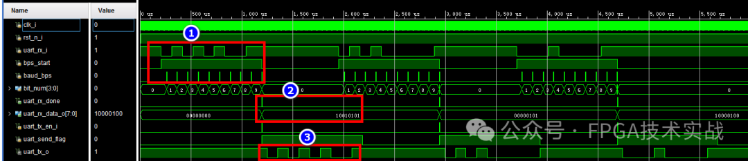
Figure 5: UART Serial Communication Simulation
In the figure, at position ①, the simulation UART receives the serial port signal uart_rx_i input data 8’b10101001, baud_bps samples at the midpoint of each bit width, and bit_num counts the number of received data bits, with data received according to LSB first;
At position ② in the figure, after completing the reception of 8 data bits, the reception complete signal uart_rx_done is generated;
At position ③ in the figure, the received data is sent through uart_tx_o according to the pre-defined transmission protocol.

Welcome to follow the FPGA technology practical WeChat account, and feel free to share!