Four Points of New Knowledge, a public account for learning, welcome to follow and communicate. Click above to follow!
Everyone knows that CIS wafers require epitaxial wafers, especially for the BSI process. But what exactly are epitaxial wafers? The term epitaxy is closely related to the specific applications of devices. To meet the needs of different devices, various epitaxial growth methods have been developed. The word “Epitaxy” comes from Greek, where “epi” means “on top of” and “taxy” means “ordered arrangement.” The basic definition of epitaxy is: growing a single crystal film on a single crystal substrate, with the crystal axes of the growing layer aligned with those of the substrate. If the epitaxial layer is made of the same material as the substrate, it is called homoepitaxy; if the materials are different, it is called heteroepitaxy.
Depending on the method of raw material supply, epitaxy can be divided into vapor-phase epitaxy, liquid-phase epitaxy, and solid-phase epitaxy. Among these, vapor-phase epitaxy can be further divided into chemical vapor deposition and physical vapor deposition. Figure 1 shows the classification of epitaxial technologies.
According to the design requirements of the device, it is common to grow epitaxial layers with different impurity concentrations on the substrate. For example, growing a low concentration p-type epitaxial layer on a high boron-doped p⁺ type substrate (p/p⁺ structure) is very beneficial for improving the performance of CMOS devices. However, in this process, impurities from the substrate may enter the epitaxial layer, causing an “auto-doping” effect. To suppress auto-doping, it is often necessary to increase the thickness of the p-type epitaxial layer. On the other hand, if a specified concentration epitaxial layer is grown on a low concentration p⁻ type substrate (p/p⁻ structure), the epitaxial layer can be thinner than the p/p⁺ structure, thus reducing costs, but the downside is that it has poorer defect capture performance.
The quality of the substrate used for epitaxial growth significantly affects the quality of the resulting single crystal layer. It is especially important to avoid defects, dust, impurities, or contamination on the substrate surface before growth, so the substrate must be thoroughly treated and cleaned. Additionally, the natural oxide film present on the substrate surface can lead to a decrease in the crystallization quality of the epitaxial layer. To remove the natural oxide film, surface treatments such as hydrogen reduction in the growth furnace, halogen gas etching, or vacuum annealing are usually required.
For commonly used vapor-phase epitaxy techniques, to obtain high-quality epitaxial layers, the following conditions must typically be met: the substrate must have a complete single crystal structure, a clean surface, a high epitaxial growth temperature, and a growth rate that is not too fast. These requirements are crucial for yield and even for the performance parameters at the device level. If these conditions are not met, the yield of subsequent chips will also be significantly affected.
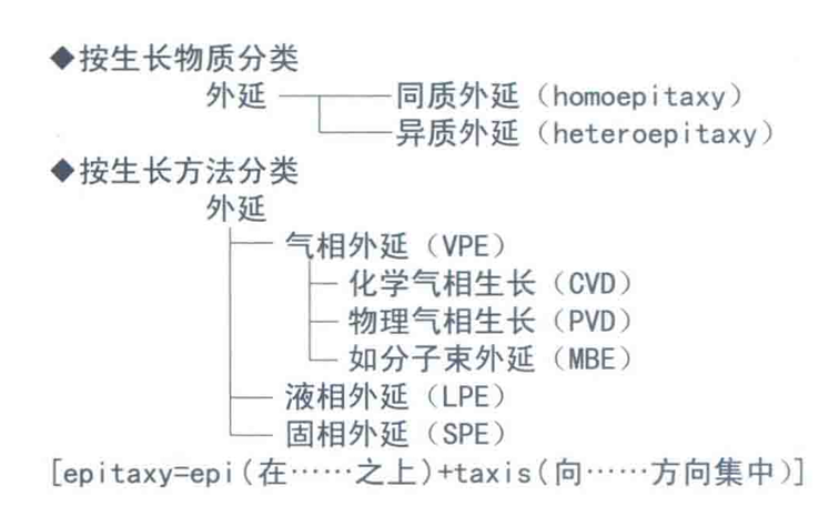
Figure 1: Classification of Epitaxial Technologies
The demands of these special devices require different materials, which are also cost optimizations made for the enhancement of device performance.
Four Points of New Knowledge is a public account for learning, welcome to follow and communicate.Five minutes a day, learning adds fun. Believe in the power of persistence. PS: Advertisement, if you’re tired of studying, how about a cup of coffee?