Follow and star our public account for exciting content
Source: Content from http://www.cnblogs.com/IClearner/, Author: IC_learner, thank you.
Today, let’s talk about low power design. This low power design is basically at the introductory level, which means it is mostly explained from a theoretical perspective. You could say it is based on what is written in books, not only from a theoretical standpoint but also combined with EDA tools to explain how to perform low power design. Now, let’s take a look at the main content of this topic:
-
Objectives of low power design
-
Composition/types of power consumption
-
Power consumption analysis and process – using EDA tools
-
Low power design and optimization
1. Objectives of low power design
1. Demand for portable devices
Electronic products play an extremely important role in our lives, and portable electronic devices are one of them. Portable devices require battery power and consume battery energy. Given the same energy supply, products designed for low power consumption can operate for a longer time. Time is life, so low power design is very important. Portable devices need low power components; for example, if a mobile phone takes two hours to charge but only allows for five minutes of talk time, who would still buy your phone…
2. Impact on reliability and performance
Devices consume electrical energy, which generates heat; the more energy consumed, the more heat produced. Increased heat can lead to greater thermal noise, which affects the normal operation of components, causing circuits to malfunction. An increase in heat may cause a circuit designed to operate at 1G to only function at 500M, which affects speed. This is most commonly seen with mobile phones; when a phone heats up, it starts to lag.
3. Impact on cost
If low power design is not carefully considered, it may lead to increased costs later on, thereby raising the overall system cost. For example, without low power design, heat generation may increase, necessitating considerations for heat dissipation during packaging, which raises packaging costs. Additionally, if the chip’s power consumption is too high during system assembly, external cooling solutions may need to be added, such as a fan, or even liquid cooling for devices that generate significant heat. This increases assembly costs. Therefore, it is crucial to implement low power design from the initial stages of design.
Of course, besides the three points mentioned above, there are many other reasons for low power design. Here, I have listed three points mainly to illustrate that low power design is one of the future trends in digital IC development, and we should pay attention to low power design.
2. Composition/types of power consumption
This section mainly introduces the composition of power consumption and the power models in the technology library. The composition of power consumption can be described from two perspectives: one is from the types of power consumption, and the other is from the system architecture. In the design process, we often discuss power consumption from the perspective of types; the power models in the technology library mainly provide specific and supplementary explanations of power consumption types. Now, let’s take a look at the engineering of power consumption.
1. Composition of power consumption – classified by type
Low power consumption can be classified into three main types: dynamic power, static power, and surge power. In this first point, I will provide a brief introduction, and in the later third point, I will introduce it in conjunction with the technology library.
(1) Dynamic power
Dynamic power includes: switching power (also known as flip power) and short-circuit power (also known as internal power).
① Switching power
In digital CMOS circuits, power is consumed when charging and discharging the load capacitance. For example, in the following CMOS NOT gate:
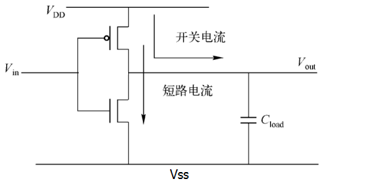
When Vin = 0, the PMOS above is on, and the NMOS below is off; VDD charges the load capacitance Cload, and after charging, the output level Vout is high.
When Vin = 1, the PMOS above is off, and the NMOS below is on, discharging the load capacitance through the NMOS, and after discharging, the output level Vout is low.
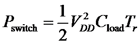
This on-off change, the charging and discharging of the power supply, forms the switching power. The calculation formula for switching power Psitch is
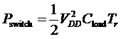
In the above formula, VDD is the supply voltage, Cload is the equivalent capacitance load of the subsequent circuit, and Tr is the input signal’s toggle rate (we will introduce toggle rate in the later third point).
Generally, the signal toggles twice on average within one cycle, once on the rising edge and once on the falling edge, meaning Tr = 2f. Therefore, the average power consumption is:
Pdynamic = Vdd * Vdd * CL * f
We do not need to delve into how this formula is derived; knowing that this power consumption is calculated this way is sufficient. If interested, one can explore further.
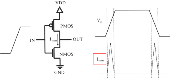
② Short-circuit power
Short-circuit power, also known as internal power, occurs because the signal transition cannot be instantaneous. Therefore, PMOS and NMOS cannot always be in one cutoff while the other is on; there is always a period when both PMOS and NMOS are on simultaneously, creating a path from the power supply VDD to ground VSS, resulting in short-circuit current, as shown in the following inverter circuit diagram:
The calculation formula for short-circuit power Pshort is as follows:
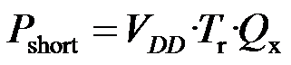
In the above formula, Vdd is the supply voltage, Tr is the toggle rate, and Qx is the charge flowing from the power supply to ground during one transition.
From this, we can see that dynamic power mainly consists of switching power and short-circuit power; among them, switching power accounts for a large proportion of dynamic power. From the two formulas above, we can see that dynamic power is mainly related to the supply voltage, toggle rate, and load capacitance.
(2) Static power
In CMOS circuits, static power is mainly caused by leakage current, as shown in the following diagram:
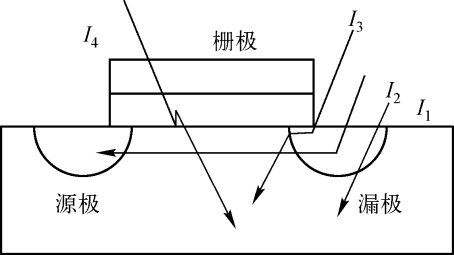
Leakage current consists of the following parts:
-
PN junction reverse current I1 (PN-junction Reverse Current)
-
Sub-threshold leakage current I2 between the source and drain (Sub-threshold Current)
-
Gate leakage current, including induced gate leakage current I3 between the gate and drain (Gate Induced Drain Leakage)
-
Gate tunneling leakage current I4 (Gate Tunneling)
Generally, leakage current mainly refers to gate leakage current and sub-threshold current (after entering ultra-deep submicron technology, tunneling leakage current becomes one of the main currents). Therefore, I will briefly introduce these two types of currents.
Gate leakage power: After applying a signal to the gate (i.e., gate voltage), there exists capacitance between the gate and substrate, thus current flows between the gate and substrate, resulting in power consumption.
Sub-threshold current: When the gate voltage is below the conduction threshold, leakage current still flows from the FET drain to source. This current is called sub-threshold leakage current. In narrow transistors, when the drain and source are close together, sub-threshold leakage current occurs. The narrower the transistor, the larger the leakage current. To reduce sub-threshold current, high-threshold devices can be used, and threshold voltage can be increased through substrate bias, which falls under low power design; we will discuss this in the later low power design section.
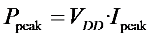
Static power calculation formula is as follows, where Ileak is the leakage current (Ipeak should be Ileak):
Static power is often related to the technology used, which we will further discuss in the third section.
(3) Surge power
Surge power is the power caused by surge current. Surge current refers to the maximum current flowing through the device when it is powered on or awakened; therefore, surge current is also known as startup current. Generally, surge power is not our main concern, so I will just mention that this type of power exists.
2. Composition of power consumption – classified by structure
Previously, we classified power consumption by type; here we classify it by structure, which means categorizing based on the device’s structure or composition (taking SoC as an example). The main categories are: clock tree power, processor power, memory power, other logic and IP core power, and input/output pad power. In different applications and devices, the proportions of these power types vary, but clock tree, processor, and memory account for the vast majority of power consumption, which is important to note.
3. Power models in the technology library
Having introduced the composition of power consumption, in this section, we will explain power consumption (composition) in conjunction with the technology library and provide examples of power calculation.
(1) Power information and calculations in the technology library
① Calculation of switching power and related library information
As we learned earlier, switching power is mainly caused by charging and discharging the output capacitance. The technology library contains information related to switching power, as shown below:
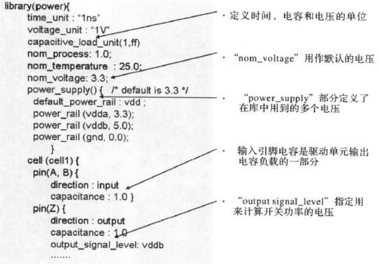
Switching power can be expressed using switching energy and toggle rate: P = E·Tr = C·v^2·T2, where switching energy E = CV^2. We will explain toggle rate later; it is placed later for immediate use and to help everyone understand the composition of power consumption.
② Internal power/short-circuit power and related library information
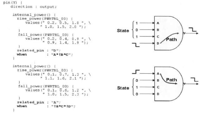
We have introduced internal power earlier; here I will reiterate that short-circuit power/internal power occurs during the transition of a unit (for example, an inverter unit) from 0 to 1 or from 1 to 0, when both the PMOS and NMOS are on simultaneously. This is not due to unit damage but rather the short-circuit power generated during normal operation. The technology library contains the short-circuit power of the unit, which is pre-processed by characterization tools and stored in the power lookup table of the technology library. This means we can obtain internal power from the relevant parameters of internal power in the technology library. The internal power information in the technology library is as follows:
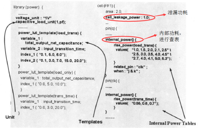
The internal power of the unit is related to its transition time and output capacitance load. Based on the input transition time and output capacitance size, we can look up the rising power and falling power in the technology library, and then calculate the total internal power using the following formula:
Pi = (rising power + falling power) · 0.5 · Tr
It should be noted that the power model in the technology library is quite accurate; power is state-dependent and path-dependent, i.e., state dependent path dependent (SDPD).
③ Static power/leakage power and related library information
Static power/leakage power is also pre-processed by characterization tools and stored in the technology library. The static power information in the technology library is as follows:
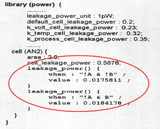
Static power is related to the state of the unit, meaning that the power consumption varies depending on the input (or unit) state. By looking up the state, we can obtain the corresponding static power.
(2) Calculation examples
① Toggle rate
We have been discussing toggle rate; what exactly is it? Here, I will introduce it.
Toggle rate (Tr): The number of signal transitions (including clock, data, etc.) per unit time. As shown in the following diagram:
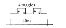
The signal toggled four times in 40ns, so the toggle rate is: Tr = 4/4ns = 0.1GHz
② Example of dynamic power calculation
From the previous sections, we know that when calculating dynamic power, we use the toggle rate. The expression for switching power is:
The expression for internal power is:
Pi = (rising power + falling power) · 0.5 · Tr
Now, we will use the toggle rate and power information from the technology library to calculate the dynamic power of the circuit shown in the following diagram:
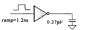
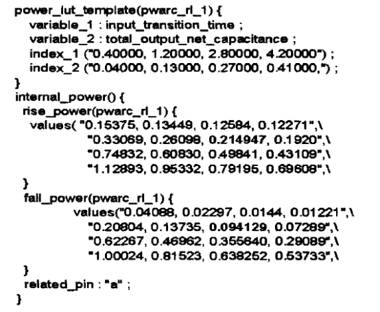
The technology library information is as follows:
Calculation of switching power in dynamic power:
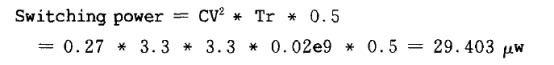
According to the formula, we can directly calculate the switching power to be: 29.403uw
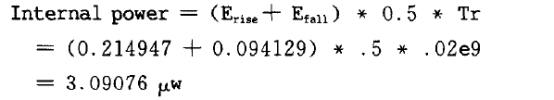
Dynamic power’s short-circuit power/internal power:
Pi = (rising power + falling power) · 0.5 · Tr
According to the formula, we first need to look up the technology library to find the rising (edge) power and falling (edge) power. The input transition time is 1.20000, and the output capacitance load is 0.270000, so the corresponding rising power and falling power are: 0.214947 and 0.094129, respectively. Therefore, the total internal power is:
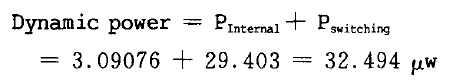
Thus, the total dynamic power is:
③ Other considerations
The power of the unit may be related to its state and path, as shown in the diagram below:
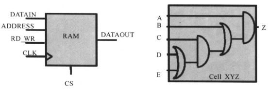
The left diagram shows a RAM unit, where the power is different in read and write states. Additionally, the power consumption of the unit varies in different operational modes.
The right diagram illustrates different paths from input to output; different paths result in different power consumption.
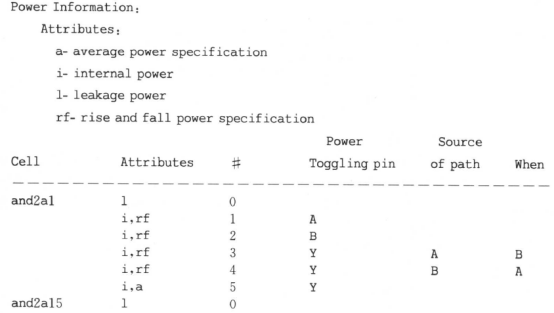
The technology library contains power descriptions for different states and paths, known as SDPD descriptions, as shown in the diagram below:
We can also use the command report_lib slow -power in EDA tools to list the power information in the library:
*Disclaimer: This article is compiled from the internet, and the copyright belongs to the original author. If there is any error in the source information or infringement of rights, please contact us for deletion or authorization matters.
‧‧‧‧‧‧‧‧‧‧‧‧‧‧‧‧‧ END ‧‧‧‧‧‧‧‧‧‧‧‧‧‧‧‧Recommended Reading:
ZYNQ Learning | Collection
Little Mo has something to say | Collection