
With the rapid development of algorithms such as deep learning, large models, and generative artificial intelligence, the advancement of artificial intelligence has placed higher demands on chip computing power, leading to the emergence of AI-specific chips that meet these higher computing requirements.

In February 2025, Huawei launched a groundbreaking product called the “Ascend DeepSeek Large Model Integrated Machine,” which deeply integrates the Ascend high-performance computing base with the full range of DeepSeek models, meeting the needs of various scenarios such as language understanding and image analysis, providing enterprises with a one-stop AI solution. This new product has sparked widespread attention in the industry regarding domestic chips. With the rapid development of large models and generative artificial intelligence algorithms, the demand for computing power is also increasing rapidly. Traditional central processing units (CPUs) can no longer meet these computing demands, driving the rapid development of artificial intelligence chips (AI chips).
In the field of artificial intelligence, the importance of chips is self-evident; they serve as the foundation for AI computation, providing powerful computing support for various intelligent applications. For a long time, NVIDIA’s GPUs (graphics processing units) have dominated the AI chip market due to their excellent parallel computing capabilities and mature CUDA development platform, almost becoming synonymous with AI computation. However, with technological advancements and intensified market competition, dedicated chips such as Huawei’s NPU (Neural Processing Unit) and Google’s TPU (Tensor Processing Unit) have begun to emerge, attempting to break NVIDIA’s GPU monopoly. Today, let us discuss the stories of these three “players” from the perspective of patents and technology.

NVIDIA GPU:
The “Big Brother” of the AI Chip Market
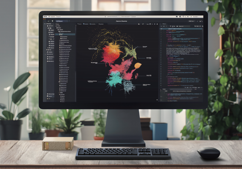
NVIDIA’s GPUs were originally designed for graphics rendering, but with the rise of deep learning, it was discovered that the parallel computing architecture of GPUs is also suitable for a large number of matrix operations. Thus, NVIDIA seized this opportunity, continuously optimizing its GPU architecture and launching dedicated GPU series for AI computation, such as Tesla and A100. These GPUs not only have strong computing power but also provide a wealth of development tools and libraries through the CUDA platform, enabling developers to easily implement various complex AI models on GPUs. With these advantages, NVIDIA occupies over 80% of the AI chip market, becoming the undisputed “big brother.”
NVIDIA Project Digits product Image/NVIDIA official website
Due to its dominance in the GPU field, NVIDIA focuses on deepening its efforts in the traditional GPU chip area, with relatively little involvement in the AI-specific chip field. Based on the key core technologies of AI-specific chips, extracting main keywords and classification numbers, and constructing search queries in the Incopat patent database for patent data retrieval, it can be seen that NVIDIA’s related patent applications rank eighth globally, far below Huawei and on par with the application volumes of most other IT companies, indicating that AI-specific chips are not a primary focus for NVIDIA.
From its product line, at the latest International Consumer Electronics Show (CES 2025), NVIDIA launched the new GB10 Grace Blackwell chip and the Project Digits equipped with the GB10 super chip, primarily supporting AI training and inference tasks in data centers, enabling large-scale deep learning, such as generative AI and large language models. NVIDIA continues to iterate its products in a traditional manner, aligning itself with the new development direction of AI technology.
New Opportunities in the AI-Specific Chip Market
Due to NVIDIA’s high market share in the GPU market, some large technology companies have begun to develop their own AI-specific chips to reduce reliance on a single supplier’s technology. AI chips can be technically divided into two categories: general-purpose chips and dedicated chips. General-purpose chips are like “all-rounders,” suitable for high-computing scenarios, such as common GPUs, but they have lower efficiency and higher power consumption when handling complex tasks like deep learning. In contrast, dedicated chips are like “special forces,” specifically designed for deep learning tasks, with common dedicated chips including video processing units (VPUs), tensor processing units (TPUs), deep learning processors (DPU), and neural processing units (NPU). With the rapid development of AI technology, dedicated chips are becoming an important force driving industry progress.
Google TPU:
Custom Chips Born for Deep Learning
TPU chips are processing units launched by Google specifically designed to accelerate tensor computations. Unlike GPUs, TPUs were tailored from the beginning for machine learning tasks, with their architecture and overall design focused on efficiently executing deep operations such as matrix multiplication.
There is a vivid metaphor to illustrate the difference in usage scenarios between TPUs and GPUs: if it is raining outside, you do not need to know how many raindrops fall per second; you only need to know whether it is heavy or light rain. Similarly, neural networks typically do not require 16/32-bit floating-point numbers for precise calculations; 8-bit integer predictions may suffice. Faced with an already mature GPU market, Google devised a new approach: during neural network inference, appropriately lowering computational precision does not affect deep learning results, while model compression can significantly increase inference speed and reduce resource consumption to meet diverse AI model training needs. The key element in TPU is the matrix multiplication unit, which operates in a pulsed array form to perform instruction calculations, referred to as the “heart” of the TPU.
Looking at Google’s product line, TPU chips have undergone six updates and iterations. As early as 2015, Google launched TPUv1, focusing on proposing the pulsed array architecture. Google first publicly introduced the TPU concept diagram in 2016 and detailed the TPU chip structure in a paper at a top international conference in 2017. In 2015, Google applied for its first core patent related to the pulsed array, revealing the important architecture and core functional modules of TPU, disclosing how to execute multiple matrix operations in parallel, fully utilizing the pulsed array in neural networks, and providing illustrations that are essentially the same as the existing TPU chip framework, with its family being cited 166 times, highlighting its significance.
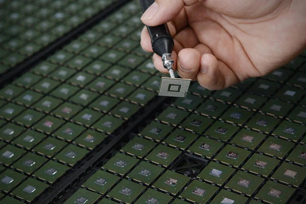
In its early days, Google kept TPU chip-related technologies more as trade secrets, focusing on global patent layout for core technologies. In the early application scenarios, TPU chips were mainly used in internally developed products such as the AlphaGo robot. Later, by deploying TPUs on Google Cloud Platform, Google not only met its massive AI computing needs but also provided strong AI computing support for cloud customers. Thus, in the early stages, Google primarily aimed to meet internal demands such as cloud services and search engines, reducing reliance on hardware suppliers like NVIDIA and achieving technological autonomy. Subsequently, Google made multiple iterations and upgrades to the TPU chips in terms of energy efficiency and performance to meet the increasing computational demands and support more complex AI tasks. In terms of patent technology, Google also holds numerous patents on TPU technology, notably with high family counts, achieving a global layout of core technologies. These patents cover various aspects such as chip design, algorithm optimization, and system architecture, aimed at improving instruction computation efficiency and reducing energy consumption. To meet the needs of emerging computational models like large models, Google has recently deployed multiple patents focusing on data compression arrays and performance optimization of acceleration processors. However, when it comes to Google’s most eye-catching innovative achievements, AI applications like Gemini are clearly more appealing to the public. The outstanding performance of the Gemini model relies heavily on the support of the fourth and fifth generation TPU technologies.
In May 2024, Google released the sixth-generation TPU chip, Trillium, which achieved significant breakthroughs compared to the previous TPU v5e—the peak computing power increased by over 4.7 times, and energy efficiency improved by over 67%. Google chose to provide the computing power of Trillium TPU to customers through its cloud service platform. Notably, Google does not directly sell TPU chips. From its strategy, Google focuses on building a strong AI ecosystem. Analysts point out that if Google competes with generative AI companies like OpenAI in the large model field while simultaneously facing off against NVIDIA in hardware, it may find itself in a dilemma of being “attacked from both sides.” Directly confronting NVIDIA may not be the best choice for Google at this time. However, the TPU chip, with its excellent cost-performance advantage, has attracted many technology companies, including Apple, and numerous startups to deploy their AI application models on this platform. With the TPU chip, Google has not only achieved technological autonomy but has also quietly encroached on NVIDIA’s market share. Furthermore, Google’s carefully constructed patent network has formed a tight technological protection barrier, providing strong technical support for competition in the AI-specific chip field.
Huawei NPU:
The Innovative Journey of the Da Vinci Architecture
Huawei’s NPU (Neural Processing Unit) stands out with its unique Da Vinci architecture, which is specifically tailored for AI computation. The built-in 3D Cube computing engine is known as a “super computing engine,” significantly improving the chip’s efficiency in handling deep learning tasks through innovative matrix computation methods. Compared to traditional CPUs and GPUs, the performance of the same chip area is cross-domain enhanced while significantly reducing energy consumption.
The development path of Huawei’s NPU can be described as a “comeback in adversity.” Unlike NVIDIA and Google, Huawei faced external technological blockades from the U.S. CHIPS and Science Act and carved out a path of independent innovation. No advanced processes? No ready-made IP cores? Then create them yourself! This “forced” independent research and development situation has instead led to a breakthrough legend for domestic AI chips, exploring a path of autonomous and controllable AI accelerator development.
From a patent perspective, Huawei’s innovative strength is remarkable. Since 2017, with the rapid development of global artificial intelligence technology, algorithm innovations have significantly propelled the progress of the chip industry. Huawei has keenly seized this “opportunity” and rapidly laid out patents related to AI-specific chips, with a noticeable increase in application volume. By 2021, the number of related patent applications peaked, akin to taking a head start in the AI race, successfully occupying a favorable position.
In terms of its product line, at the end of 2018, Huawei first introduced the Ascend 910 and Ascend 310 AI chips, marking the official landing of Huawei’s AI-specific chips. At the same time, Huawei conducted meticulous patent layouts, reflecting a strong awareness of patent protection, closely integrating patent applications with product development. This strategy of “patents and products running in parallel” not only enhances the conversion and utilization value of patents but also provides a tight patent protection network for Huawei’s competition in the AI-specific chip field, fully embodying the concept of “technology prioritizing patents.”
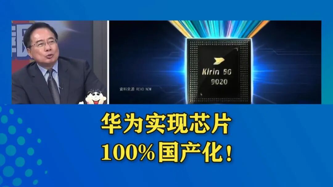
As matrix operations are the “pillar” of computing power, Huawei has invested significant effort in improving their efficiency. As early as 2017, Huawei applied for a patent related to matrix multipliers, which has been cited 62 times and covers countries and regions such as the U.S., South Korea, Japan, Italy, and Europe. This patent is a key focus for Huawei’s layout and lays a solid foundation for subsequent patent applications, demonstrating Huawei’s determination to target the global market from the outset. On this basis, Huawei continues to delve into the optimization of matrix and tensor operations, indicating that Huawei’s technological layout in this field is becoming increasingly refined. In the last two to three years, Huawei has made several new moves in the AI chip field, deploying a series of initiatives around vector operations in compressed formats and improving operator computing efficiency, especially in the area of underlying instruction optimization, forming a tight patent protection network to ensure product stability.
For the overall layout of AI chips and AI platforms, Huawei is also taking a step-by-step approach. In the early stages, it applied for patents related to computing accelerators, chips, and terminal products to protect the overall architecture and AI chip-based terminal products. In the mid-term, Huawei built a full-scenario AI infrastructure solution targeting “end, edge, and cloud,” and made a series of patent layouts around key technologies such as network structure and neural network accelerators. Recently, Huawei has focused on performance optimization of AI accelerators, achieving technological breakthroughs in aspects such as balanced memory access and multi-operator collaboration. Huawei’s technological evolution route in the AI-specific chip field shows a clear progression, gradually moving from the initial “foundation laying” to the “refinement” stage. From matrix operations to a full-scenario AI infrastructure ecosystem, and then to the “fine-tuning” of AI platform performance, every step taken by Huawei is both solid and forward-looking. Under the pressure of external technological blockades, Huawei did not retreat but instead successfully carved out a path of autonomous and controllable AI-specific chip development through a series of innovations and patent layouts. This not only lays a good foundation for Huawei’s own development but also provides valuable experience for the development of the domestic AI chip industry.
In terms of product lines, Huawei’s Da Vinci architecture can cover various application scenarios. The first path is as a co-processor for mobile terminals to enhance mobile computing performance. In this path, Huawei integrates the NPU chip within the Kirin mobile chip, working in collaboration with the CPU and GPU. In 2017, Huawei launched the first smartphone with an AI processor, the Mate 10 series, and subsequently iterated with the Mate 30 and Mate 40. Later, facing the “bottleneck” situation in chip technology, Huawei made a comeback in 2023 with the Mate 60, using its self-developed Kirin processor combined with the NPU chip. The second path is using the NPU chip as an inference training chip, with typical products being the Ascend series, such as Ascend 310 (for inference) and Ascend 910 (for training), as well as the Atlas series servers based on Ascend 310 and 910. Huawei builds a domestic computing power ecosystem through its AI computing framework, gaining a certain market share domestically, but still has a gap in maturity and acceptance compared to NVIDIA’s ecosystem. Overall, Huawei’s Da Vinci architecture and Ascend series computing cards set a benchmark for the development of domestic computing power technology. Looking at Huawei’s related patents, they mainly adopt a “problem-oriented” innovation path. In the face of difficulties in obtaining advanced processes due to U.S. sanctions, Huawei has formed a rich patent pool around how to achieve competitiveness under sub-optimal processes, providing breakthrough ideas for domestic enterprises in this field.
Market Competition: Challenges and Opportunities Coexist
The current AI-specific chip field presents a diversified competitive landscape, with Huawei’s NPU and Google’s TPU reshaping the industry pattern through their respective technological breakthroughs. Both companies demonstrate outstanding performance in technology and performance, posing a strong challenge to NVIDIA’s market and ecosystem development. However, NVIDIA’s dominant position in the AI chip field remains solid. With strong technical strength, a mature development platform, and a wide user base, NVIDIA continues to occupy a large portion of the market. In the field of large model training, its latest H200 GPU further strengthens its computing power advantage, consolidating its industry leadership. Currently, the AI chip market exhibits a competitive landscape of “one strong leader and many strong competitors,” with NVIDIA as the leader guiding the industry’s development. Self-developed AI-specific chips have become a necessary path for major IT manufacturers. Huawei’s NPU and Google’s TPU provide new ideas for differentiated development in response to competition, especially in the context of rapid technological iteration, enhancing market dominance through self-developed technologies.
Patent strategies have become a key dimension of competition. Leading enterprises generally adopt a three-in-one development model of “technology research and development – patent layout – ecosystem construction.” International technology giants such as Microsoft have launched the Azure Maia chip, while Amazon has strengthened AWS services through the Trainium chip. Domestic specialized enterprises like Cambricon and Biren Technology are committed to research and development layouts in the new field of AI-specific chips. With continuous technological advancements, the competition in the AI chip field will become increasingly diversified, and manufacturers will jointly promote the sustained development of the industry through technological innovation and optimization of market strategies.
(Source: “Creative World” June 2025 issue)【Click the mini-program below to purchase this issue of the magazine】
Editor: Yuan Baoping, Reviewed by: Guo Li

Previous Keywords
Silk / Chen Anying / Shared Bicycles / Old Cui / Homestays
World of Warcraft / Chen Xiangfeng / Demand Collector / Ke Jie
GOOD DESIGN / Cultural and Creative Industry Park / “Hundred Birds Facing the Phoenix”
3D Paper Cutting / Copyright / Intangible Cultural Heritage / Design Transformation
Micro Creativity / Fixed Gear / Tang Family’s Three Young Masters / Coffee

Click the card above to follow us!
