(Source: Semiconductor Industry Observation)
With the arrival of the post-Moore era, numerous popular applications such as AI, 5G, and autonomous driving are emerging continuously. The scale of chips is growing exponentially, with designs featuring billions or even tens of billions of gates becoming commonplace. As chip size increases and process nodes advance, the costs of tape-out are also rising sharply. To improve the success rate of tape-out, EDA verification has become an essential part of high-end chip design, spanning the entire process from design to mass production. Verification consumes the most time and resources throughout the chip development process and faces numerous technical challenges. How to address the verification pain points of large chips has become a focal point for chip design companies.

1. Why EDA Verification is Crucial
Today, chip design software has gone through more than 60 years of extensive development, evolving from CAD for drawing assistance to CAE for simulation and verification, and finally to modular automated tools known as EDA. EDA, as a fundamental tool for integrated circuit design, has played a crucial role with the continuous development of large-scale integrated circuits, computer, and electronic system design technologies. It has transitioned from a supportive technology to one of the core pillar technologies of the chip industry, representing the upstream of IC design with the highest technical barriers. Without the support of EDA software, the design costs of chips would increase by dozens or even hundreds of times.
Depending on the application scenario, the use of EDA tools is mainly divided into several categories: design, verification, packaging, and manufacturing. Among these, verification covers the entire process from front-end logic design to back-end physical design and ultimately to mass production. As chip design costs continue to rise and integration levels increase, complexity has also significantly increased. Identifying all design defects and errors through verification is critical to success, making verification EDA tools a responsible entity.
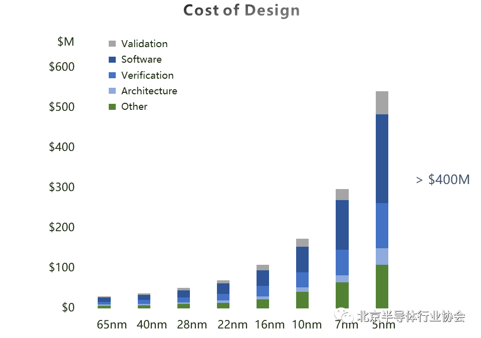
Data Source: IBS, Design Activities & Strategic Implications, July 2018
From the perspective of verification, EDA software is very complex, with high technical barriers. Most importantly, it is not only necessary to develop tools but also to continuously iterate them, requiring ecosystem and customer support to form a closed loop. Although the three major international giants have accumulated mature products in the verification market over the years, any further innovation and iteration must consider backward compatibility, which undoubtedly poses a heavy historical burden. This has also created opportunities for China to break through in the verification EDA field.
2. What are the Verification Pain Points of Large Chips
Large chips generally refer to large SoC chips, which include AI engines, CPUs, GPUs, etc., and often use advanced processes below 12nm, applied in fields such as machine learning, autonomous driving, image recognition, natural language processing, and data centers. Verifying large chips is a complex and challenging task, with the main pain points reflected in the following four aspects.
First, verification tools need to support sufficiently large chip design capacities. The tape-out costs of large chips are high, and the losses from tape-out failures are incalculable. Therefore, verification tools must keep pace with the times, be able to flexibly stack, and support ultra-large-scale chip designs while ensuring correctness and reliability.
Second, verification time needs to be minimized. Some verification tools have low levels of automation, requiring manual intervention in certain processes, which consumes engineers’ energy and affects the time to market for chips. For example, in prototype verification, due to the large size of the chip design, it needs to be partitioned for verification. The traditional method involves manual partitioning, which is time-consuming, labor-intensive, and prone to errors. Automated and intelligent partitioning methods and tools are an inevitable trend.
Third, efficient debugging tools are required. Once a problem arises, it is necessary to quickly identify the problem points in the design for debugging to achieve the fastest iteration speed. In the face of complex chips, some verification platforms have poor observability and debuggability, affecting verification efficiency. Additionally, debugging tools must continuously introduce methodological and process innovations during the iteration process, supporting not only functional debugging but also extending to power consumption, coverage, safety, and other aspects of debugging; they must support different design levels such as RTL and Gate levels, as well as transaction-level and system-level verification debugging.
Fourth, how to address the peak computing power demand before tape-out. IC companies face a peak computing power demand of 3-6 months before tape-out, requiring large memory, high-frequency computing power, and high-performance storage for chip verification. If built locally, it would consume a lot of manpower, material resources, and financial resources, and there would be limitations in computing and storage hardware resources. Coupled with time-consuming procurement and deployment processes, it makes it difficult for verification engineers to complete all expected tasks within the scheduled market launch time.
3. FPGA Prototype Verification is the Preferred Method for Large Chip Verification
In light of these pain points, FPGA (Field Programmable Gate Array) prototype verification has developed into the preferred verification method for chip companies. FPGA prototype verification is a chip functional verification method based on FPGA. It utilizes the reprogrammable nature of FPGAs to perform functional verification of chips by synthesizing RTL code onto the FPGA during the RTL code development process. The goal is to provide a repeatable logical verification platform for the chip development team before tape-out. After the chip design is finalized and before tape-out, it provides a hardware environment for the software development team to develop software functions in advance, shortening the time to market for products after tape-out. This verification environment allows chip verification and software verification to run in parallel, ensuring that the chip’s hardware and software functions are accurate in real application scenarios.
FPGA can easily achieve large-scale chip verification through cascading; and it operates at high speeds, making it particularly suitable for system-level verification. Furthermore, by cascading multiple FPGA prototype verification simulators, an EDA cloud data center can be established, utilizing cloud-based elastic computing power to meet the peak computing power demands of IC companies, effectively reducing IT investment and operational costs, improving the efficiency and quality of chip design and verification, and enabling collaborative work across regions, platforms, and devices.

4. What Advantages Does FPGA Prototype Verification Have Over Other Verification Methods?
Modern SoC chips are systems where software and hardware operate in coordination. They run complex software that works together with the chip hardware to achieve various functions. The design, development, and verification of the software system that works in coordination with the chip must proceed in sync with the chip design verification work. This is essential to ensure the correctness of chip functions, reduce the risk of chip tape-out failures, and shorten the product’s time to market.
To ensure the correctness of chip functions, a series of verification processes must be conducted after the development of the chip’s RTL code. Common digital chip verification methods include logic functional simulation, formal verification, hardware simulation, and FPGA prototype verification.
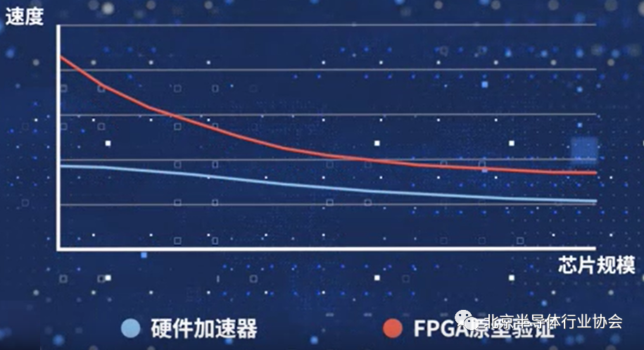
Among these common digital chip verification methods, FPGA prototype verification technology is one of the most suitable verification technologies for the collaborative functionality of chip hardware and software. The FPGA prototype verification platform can provide the necessary real physical interfaces and hardware environment for debugging chip software. This is something that logic functional simulation and formal verification cannot provide. Compared to hardware accelerators, the software running speed on FPGA prototype verification platforms is an order of magnitude faster, significantly shortening software running time and verification iteration cycles. Optimizing interface logic operating frequencies allows for integration with real devices, making parallel software and hardware development and verification possible. In the chip verification process, FPGA prototype verification technology is an essential solution for collaborative functionality verification of hardware and software, with significant irreplaceability.
Therefore, FPGA prototype verification technology, as a mainstream and mature chip verification method, has become an indispensable verification tool for digital chip companies.
5. HJ Industrial Software’s Digital Verification Full Process and Next-Generation Timing-Driven FPGA Prototype Verification System UV APS
Shanghai HJ Industrial Software Group Co., Ltd. (referred to as “HJ Industrial Software”) is a provider of high-performance industrial software and solutions based on independent innovation, focusing on full-process support for digital chip verification to achieve breakthroughs from point to surface. HJ Industrial Software has now launched a complete set of digital chip verification full-process tools, including: commercial-grade logic simulator UVS, timing-driven high-performance prototype verification system UV APS, digital functional simulation debugging tool UVD, large-scale functional verification regression testing management platform VPS, and plug-and-play hybrid prototype system-level IP verification solution HIPK. At the same time, HJ Industrial Software has also made strategic investments in Shanghai Akas, and Gubo Technology to supplement formal verification tools and semiconductor automated testing tools for the full-process verification platform.
Among them, the next-generation timing-driven FPGA prototype verification system UniVista Advanced Prototyping System (UV APS), released in June 2022, is HJ Industrial Software’s flagship product. Since its launch, it has been successfully deployed in IC companies in high-performance computing, 5G communication, GPU, artificial intelligence, and automotive electronics.
UV APS uses 4 FPGAs in a single device, which can be flexibly stacked, supporting a maximum capacity of 25 device cascades (100 FPGAs interconnected). It integrates intelligent and automated full-process compilation software APS Compiler, providing chip designers with an efficient verification method that reduces time costs during the verification phase; it also offers a rich set of FMC interface sub-cards to adapt to various interface verifications, providing ample One-Bank interconnection channels to support system expansion; combined with deep debugging solutions, it shortens testing cycles and accelerates chip market launch.
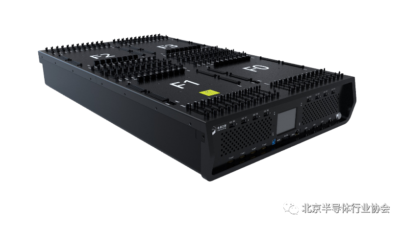
Figure: Next-Generation Timing-Driven FPGA Prototype Verification System UV APS
Innovation Point 1: Innovative Self-Developed Timing-Driven Full-Process Compilation Software APS Compiler
UV APS integrates the innovative self-developed timing-driven full-process compilation software APS Compiler, which has significant advantages in performance and automation levels.
In terms of performance: The APS Compiler features an embedded timing-driven partitioning engine that can automatically optimize solutions through a wide range of TDM Ratios, easily handling design capacities of up to 100 FPGAs, allowing logic circuits to run faster. At the same time, the APS Compiler can achieve automated timing-driven partitioning, inter-chip routing, logic localization, and MCP (Multi-Cycle Path) analysis, making the timing-driven process more complete. For typical SoC designs, the verification performance of the APS Compiler reaches over 20+ MHz, easily supporting partitioning requirements for designs exceeding 1 billion gates.
In terms of automation level: The APS Compiler can provide both fully automated and manual-guided modes based on the timing-driven partitioning algorithm of RTL Modules, helping achieve efficient verification. For design units that FPGAs cannot support, such as Multi-port Memory, multi-dimensional arrays, cross-module references (XMR), and tri-state gates, some mainstream tools in the industry require users to modify RTL code, while UV APS can achieve automated conversion.
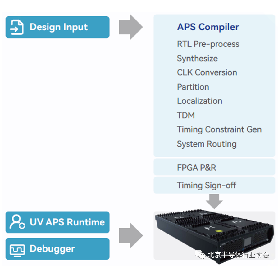
Figure: UV APS Automated Timing-Driven Compilation Process
Innovation Point 2: Diverse Debugging Methods
During the prototype verification process, debugging functionality is indispensable. Traditional FPGA prototype verification platforms are limited by their own capacity, resulting in poor observability and debuggability, while UV APS has made significant improvements in these two areas.
The signal waveform capture tool in UV APS does not occupy FPGA internal storage space. By using configurable trigger conditions, it captures internal signal waveforms of the design and stores them in external dedicated memory. It supports various logical combinations of trigger conditions, and the waveform display is clear and easy to view intuitively.
At the same time, UV APS supports FPGA chip read-back capture debugging, allowing reading of internal register values; the Back Door function enables backdoor read/write, effectively avoiding the need for users to frequently restart the system; it supports multi-FPGA, multi-trigger condition debugging, and captures signals from multiple clock domains into a single waveform file, displaying multiple waveforms in a single window. Additionally, the ECO function utilizes the incremental layout and routing features of the VIVADO tool to accelerate turnaround time. These debugging methods can greatly improve debugging efficiency, significantly shorten testing cycles, and reduce time to market.
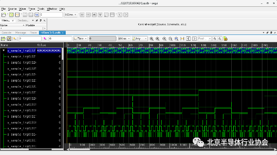
Figure: Rich Debug Functionality of UV APS
Innovation Point 3: Large Capacity and Flexible Expansion Hardware System
The FPGA prototype verification platform, as a production tool, has its hardware system’s large capacity and flexible expandability directly impacting the progress of chip verification.
In terms of capacity, the UV APS hardware system can support up to 25 device cascades.
In terms of flexibility, a single FPGA in the UV APS hardware system can support over 46 high-speed GTY transceivers, with speeds up to 28 Gbps, supporting multiple globally programmable clocks. Additionally, a single FPGA in the UV APS has over 1700 IO interfaces and provides FMC external standard expansion interfaces and One Bank connectors to meet users’ interconnection needs.
The UV APS hardware system also provides self-checking functionality and supports upper computer software control for power on and off, along with a series of safety protection measures including system status monitoring, overcurrent and overvoltage protection, and temperature monitoring.
Innovation Point 4: Solutions Adapted to Typical Application Scenarios
HJ Industrial Software’s UV APS also provides prototype verification sub-cards, Memory Models, Speed Adaptors, and rapid customization services for various industry applications; UV APS supports high-performance interface rate adaptations such as PCIe Gen5, DDR5, HBM2e, HBM3, MIPI, LPDDR5, and Gigabit Ethernet, as well as a series of solutions adapted to various typical application scenarios to meet users’ complex needs for prototype verification.
6. Large Chip Verification Computing Power Cluster Solution – Enterprise-Level EDA Cloud Data Center
Unlike traditional cloud data centers, EDA cloud data centers require the establishment of dedicated hardware simulators for large-scale chip verification. Additionally, data security is particularly important for IC companies, ensuring that chip design and verification occur in a secure working environment. Combined with flexible payment models and cloud-based elastic computing power, EDA cloud data centers can effectively reduce hardware investment costs for enterprises and improve chip verification efficiency.
For example, in a cloud data center project tailored for a semiconductor design company, HJ Industrial Software customized and deployed an enterprise-level EDA cloud data center, building a dedicated IDC machine room. Based on the client’s computing power requirements, a cloud device cluster for FPGA hardware verification was established, cascading hundreds of FPGAs to run 24/7, validating ultra-large-scale system chips for the client. It can simultaneously operate various verification scenarios, including chip design simulation cloud tasks, system-level PCB design software cloud tasks, etc., while supporting cross-regional verification teams to collaborate using cloud data center resources.
7. Conclusion
Based on the self-built EDA cloud data center and the next-generation timing-driven FPGA prototype verification system UV APS and other flagship products, HJ Industrial Software has achieved dimensional elevation and breakthroughs in solving large chip verification issues, further enhancing China’s level in the EDA verification tool field and continuously supporting the development of the domestic semiconductor design industry.
HJ Industrial Software adheres to two principles in supporting Chinese chip companies: “Customer-Centric, Product as Core Competitiveness.” EDA is a product-driven industry, and while maintaining technological and performance leadership, it is necessary to quickly grasp the true needs and pain points of design companies, developing and evolving EDA design methodologies from the front-end requirements to create better products and technologies, continuously optimizing. Upholding the corporate spirit of “Upholding Integrity and Innovation, Practicing Diligently and Far-Reaching,” HJ Industrial Software will continue to iterate and update technology to maintain product competitiveness.