RK3588 VDD_CPU_BIG0/1 Power PCB Design
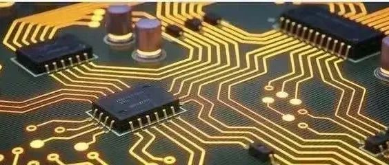
1. As shown in Figure 1, the filtering capacitor must be placed on the back of the corresponding power pin of the RK3588 VDD_CPU_BIG power pin, within the green line of the schematic. The capacitor GND PAD should be placed as close as possible to the GND pin at the center of the chip, as shown in Figure 2. The remaining decoupling capacitors should be placed as close as possible to the 3588 chip, but they need to be placed along the path of the power split source.

Figure 1 Decoupling capacitors for RK3588 chip VDD_CPU_BIG0/1 power pins in the schematic

Figure 2 Placement of decoupling capacitors on the back of the chip VDD_CPU_BIG0/1 power pins
2. Ensure that each power pin of the RK3588 chip VDD_CPU_BIG0/1 has a corresponding via next to it, and the top layer should be routed in a zigzag pattern with cross connections, as shown in Figure 3. It is recommended to use a trace width of 10 mil.

Figure 3 Routing of power pins for RK3588 chip VDD_CPU_BIG0/1
3. The copper width for VDD_CPU_BIG0/1 must meet the current requirements of the chip. The copper connected to the chip power pins must be wide enough, and the path should not be excessively interrupted by vias. The effective trace width must be calculated to ensure that the paths connecting to each CPU power PIN are sufficient.
4. When changing layers for the VDD_CPU_BIG power supply, it is recommended to use at least 12 vias of 0.5*0.3mm to reduce the voltage drop caused by layer changes. The number of GND vias for the decoupling capacitors should match the number of power vias; otherwise, it will significantly reduce the effectiveness of the capacitors.
5. The VDD_CPU_BIG current is relatively large and requires double-layer copper. The total width of the VDD_CPU_BIG power in the CPU area must not be less than 300 mil, and the width in the peripheral area must not be less than 600 mil. It is advisable to use copper pour to reduce the voltage drop caused by routing. Other signal layer change vias should not be placed arbitrarily; they must be placed regularly to allow space for power routing, which also benefits the ground layer copper, as shown in Figure 4.

Figure 4 Copper pour for RK3588 chip VDD_CPU_BIG0/1 power layer
6. The power plane will be damaged by the via solder mask. When designing the PCB, adjust the positions of other signal vias to ensure that the effective width of the power meets the requirements. In the following image, L1 is the width of the power copper of 58 mil. Due to the solder mask of the vias damaging the copper, the actual effective current-carrying width is only L2+L3+L4=14.5 mil, as shown in Figure 5.

Figure 5 Effective current-carrying width of the power
7. It is recommended to have at least 12 GND vias within a 40 mil range (center to center distance of vias) for the BIG0/1 power vias, as shown in Figure 6.

Figure 6 Placement of GND vias for BIG0/1 power
8. The recommended target impedance values for the BIG power PDN are shown in Table 1 and Figure 7:

Table 1 Recommended target impedance values for BIG power PDN

Figure 7 Recommended PDN requirements for BIG power

PCB Design Considerations for RK806 Power Solutions
PCB Design Layout and Routing Requirements for Clock Circuits

Scan to add customer service WeChat, note “Join Group” to pull you into the official technical WeChat group of Fanyi Education to exchange technical issues and experiences with many electronic technology experts~