With the increasing performance demands of chips driven by technologies such as AI, 5G, and autonomous driving, traditional packaging methods are gradually losing their advantages. An emerging technology—Hybrid Bonding—is becoming a key breakthrough in advanced packaging. It is reshaping the way chips connect, becoming the core process for high-performance computing, high-bandwidth memory (HBM), and ultra-high-layer 3D NAND products.
What is Hybrid Bonding?
Hybrid Bonding is an advanced bonding method that simultaneously connects metal layers and dielectric layers at room temperature or low temperature. It breaks through the limitations of traditional connections achieved through wires, solder balls, or bumps, relying solely on copper contacts to achieve nanoscale high-density interconnections between chips.

Hybrid bonding process: three steps to achieve strong coupling:
CMP and Surface Activation:The wafers undergo chemical mechanical polishing and cleaning to obtain an ultra-smooth, particle-free hydrophilic surface.
Pre-alignment Bonding:Two wafers are closely bonded at room temperature, forming an initial SiO₂—SiO₂ bond.
Thermal Annealing:Annealing promotes the interdiffusion of copper atoms, achieving permanent Cu—Cu connections.
This structure of metal + dielectric dual-layer contact shortens the transmission distance of electrical signals between chips, reduces latency, and significantly enhances performance.
Advantages of Hybrid Bonding
Hybrid Bonding is not a minor upgrade; it represents a comprehensive leap over traditional connection methods.
Hybrid Bonding fundamentally changes the internal communication structure of chips, resulting in faster computing speeds, lower power consumption, and more efficient heat dissipation.
01
Logic Chips: Performance Improvements Multiply
For example, according to AMD’s experimental data, compared to thermal compression bonding, under Hybrid Bonding, the interconnection density of logic chips increases by 15 times, signal speed increases by 11.9 times, bandwidth density increases by 191 times, and energy consumption per bit decreases by 20 times.
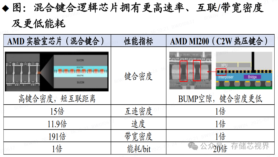
Hybrid Bonding fundamentally changes the internal communication structure of chips, resulting in faster computing speeds, lower power consumption, and more efficient heat dissipation.
02
Memory Chips: The Acceleration Engine for HBM and NAND
In the HBM Field: According to IEEE data, Hybrid Bonding allows for a higher stacking layer count in HBM chips, reducing thermal resistance by 20%, dynamic power consumption by 17%, and improving signal integrity by 20%.
In the 3D NAND Field: Taking Yangtze Memory’s Xtacking as an example, the peripheral circuits and memory cells are processed separately and then integrated through Hybrid Bonding, significantly enhancing storage transmission speeds, with Xtacking boosting NAND’s I/O speed to 3.0Gbps.
Accelerating Industrialization: The Battle Among Giants
The market potential for Hybrid Bonding is enormous. According to BESI’s forecast, by 2030, the demand for Hybrid Bonding equipment will reach 2.8 billion euros, exceeding 1,400 units, with the domestic market expected to enter a golden explosive period.
01
International Giants: BESI, EVG, SUSS, etc. Take the Lead
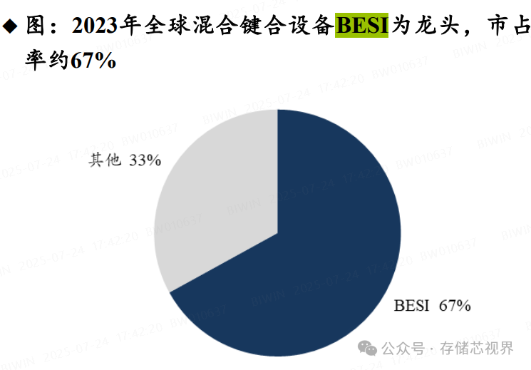
BESI: Holds a market share of 67%, launching high-precision equipment such as the 8800 Ultra, serving HBM, AI chips, SoC packaging, etc.
EVG: Focuses on wafer-level Hybrid Bonding systems ComBond, supporting various bonding materials with world-leading precision.
SUSS: Launched the XBS300 series, compatible with glass, metal, and multi-layer packaging.
02
Chinese Manufacturers: From Catching Up to Running Alongside
Tuojing Technology: Launched the first domestically produced mass-production W2W Hybrid Bonding equipment “Dione 300”, with the pre-treatment equipment “Propus” achieving repeat orders.
Maiwei Co., Ltd: Precision has reached ±100nm, aiming to benchmark against international leader BESI, with plans for multiple devices.
Chipwise (Bai’ao Chemical): Equipment has begun shipping and is entering the client verification stage.
The breakthroughs of these companies indicate that the domestic substitution of Hybrid Bonding is moving from possibility to reality.