Many modern NAND flash devices now adopt a new architecture that integrates the interface, controller, and storage chips into a common ceramic layer. We call this a monolithic structure encapsulation.Until recently, all storage cards, such as SD, Sony’s MemoryStick, MMC, etc., contained a very simple ‘classic’ structure with separate components—a controller, a PCB, and NAND memory chips in a TSOP48 or LGA-52 package. In this case, the entire recovery process is quite simple—we just unsolder the memory chip, read it directly with PC-3000 FLASH, and prepare it similarly to a regular USB flash drive.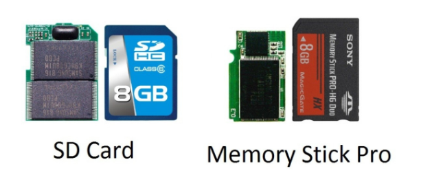 But what do we do if our storage card or UFD device is based on a monolithic encapsulation architecture? How can we access the NAND memory chip and read data from it?
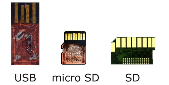
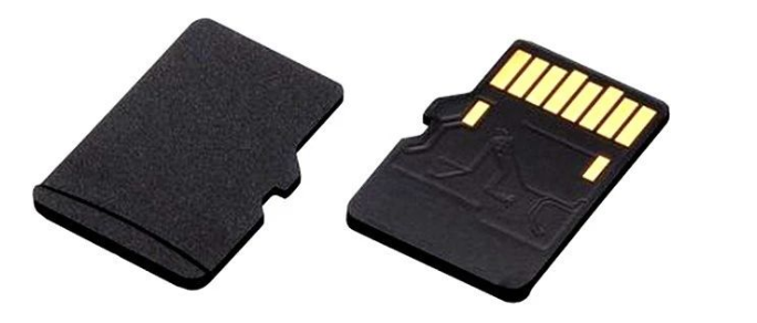
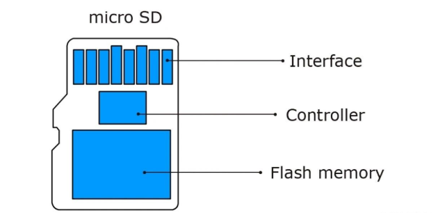 Basically, in this case, we should try to find special technical pins at the bottom of our monolithic encapsulated device by removing the ceramic layer coating.
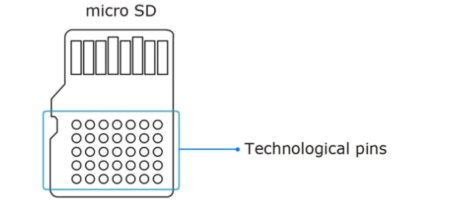 Before we start handling monolithic FLASH data recovery, we should warn you that the entire process of soldering monolithic FLASH devices is complex and requires good soldering skills and special equipment. If you have never tried soldering monolithic FLASH devices before, it is better to practice your skills on some unimportant accessories on the device. For example, you can buy a few of them to test your preparation and soldering skills.Below is a list of necessary equipment:A good optical microscope, x2, x4, x8 zoom;USB soldering iron with a very thin soldering tip, very sharp soldering tip;Double-sided tape;Liquid flux;BGA flux;Hot air gun (e.g. Lukey 702);Rosin;Wooden toothpicks;Alcohol (over 75% purity);Copper wire with a diameter of 0.1 mm, enameled wire;Jewelry-grade sandpaper (1000, 2000, 2500 grit (the higher the number, the finer the sand));BGA solder balls of 0.3 mm;Tweezers;Sharp surgical knife;Blueprints and pin allocation schemes;PC-3000 Flash PCB adapter;
When all the equipment is ready for soldering, we can start production.
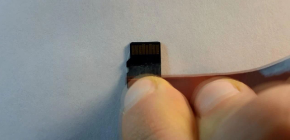
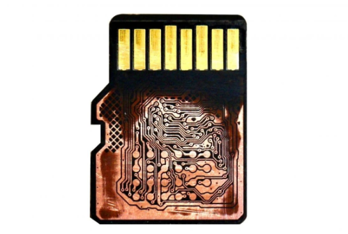
First, we use our monolithic FLASH device. In our case, it is a small microSD card. We need to fix this card to the table with double-sided tape. Next, we start removing the ceramic layer from the bottom. This operation takes some time, so you should be very patient and careful. If you damage the pin layer, data recovery will be impossible!We start with coarse sandpaper (the largest grit size) – 1000 or 1200.
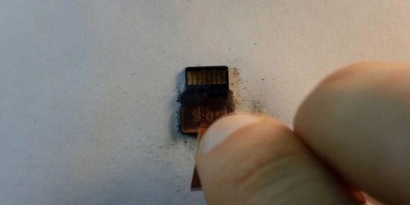
 When the first large part of the coating is removed, it is necessary to switch to finer sandpaper – 2000.
 Finally, when the copper layer of the contacts becomes visible, we should use the finest grit size – 2500.
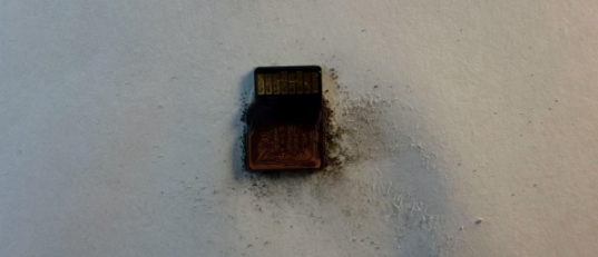 If you perform all operations correctly, you will end up with something like this:
 The next step is to search for the pins in our global solution center.To continue using the entire block, we need to solder 3 groups of contacts:
-
Data I/O contacts: D0, D1, D2, D3, D4, D5, D6, D7;
-
Command contacts: ALE, RE, R/B, CE, CLE, WE;
-
Power contacts: VCC, GND.
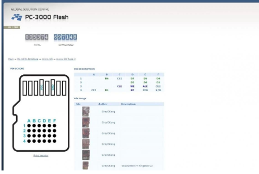
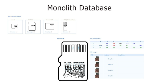 First, you need to select the category of the monolithic FLASH device (in our case, the microSD card), then you must select the compatible pin arrangement (in our case, type 2).
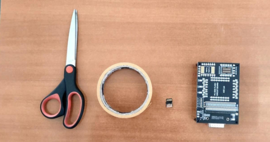
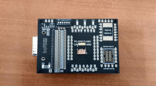
 Then we should fix the microSD card onto the circuit board adapter for easier soldering.
 It is a good idea to print out the pin arrangement scheme of the monolithic FLASH device before soldering. You can keep the scheme next to you so that when you need to check the pin array, it is right in front of you.
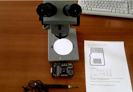 We are ready to start the soldering process! Make sure your workstation has enough light!Using a small brush, apply some liquid flux on the microSD pin contacts.
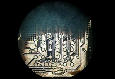
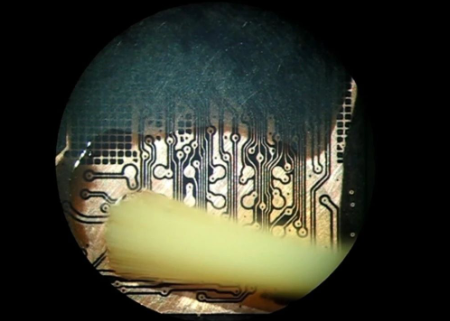 With the help of a wet toothpick, we should place all the BGA solder balls on the copper pin contacts marked on the pin arrangement scheme. It is best to use BGA solder balls that are about 75% of the contact diameter. The liquid flux will help us secure the BGA balls to the surface of the microSD card.
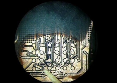
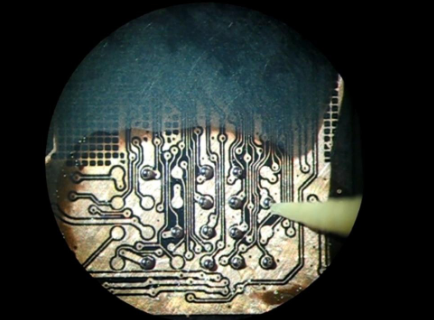 Once all the BGA solder balls are placed on the pins, we should use the soldering iron to melt the solder. Be careful! Perform all actions gently! To melt, lightly touch the BGA solder balls with the soldering iron tip.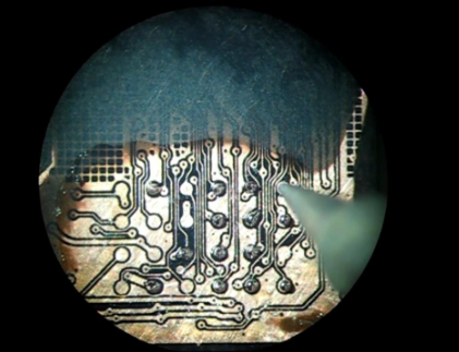
After all the BGA solder balls have melted, you need to place some BGA flux on the contacts.
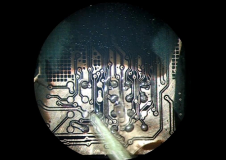 Using a hot air gun, we should heat our pins to +200C. The BGA flux helps to distribute heat among all BGA contacts and carefully melt them. After heating, all contacts and BGA solder will take on a hemispherical shape.
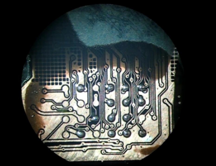 Now we should remove all traces of flux with the help of alcohol. You need to sprinkle it on the microSD card and clean it with a brush.
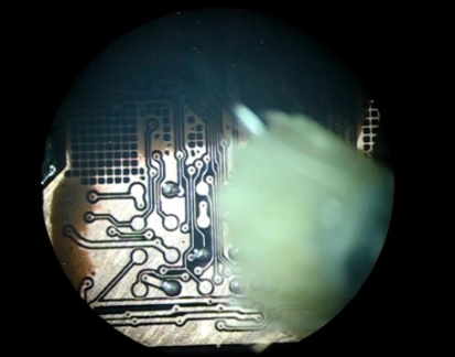
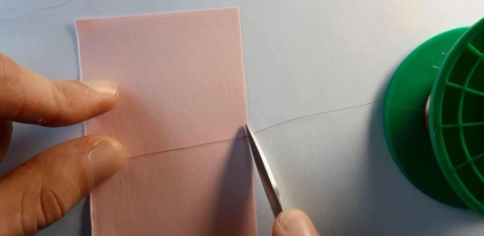
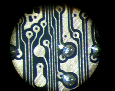 The next step is to prepare the copper wires. Their lengths should be the same (about 5-7 cm). To cut the wires to the same size, we recommend using a piece of paper as a length measuring tool.
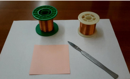
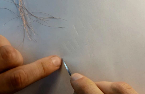
 Next, we should use a surgical knife to remove the insulation paint from the wire. Slightly scratch them from both sides.
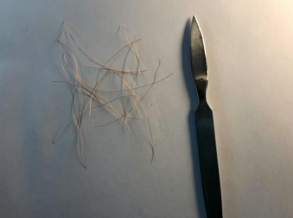
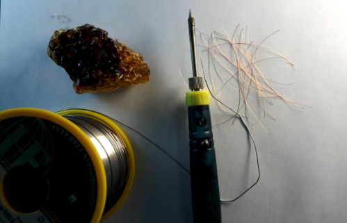
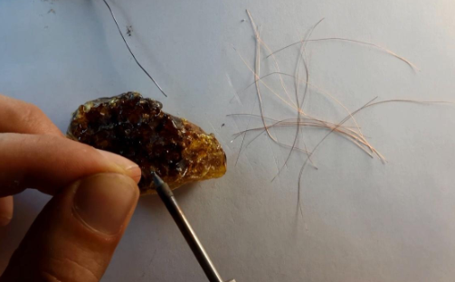
 The final stage of preparing the wires will be the tinning process with rosin for better soldering.
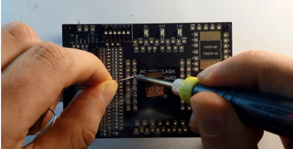
 Now we are ready to start soldering the circuit to our circuit board. We recommend starting the soldering from the side of the circuit board and then, with the help of a microscope, continue soldering the other side of the wire to the monolithic device.
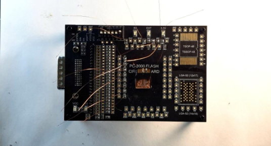 Finally, all wires are soldered to the circuit board, and we are ready to start soldering the wires to the microSD card using the microscope.This is the most complex operation and requires a lot of patience. If you feel tired – take a break, eat something sweet, drink a cup of coffee (sugar in the blood will help keep your hands steady). After that, start soldering.For right-handed people, we recommend holding the soldering iron in the right hand and using tweezers to hold the copper wire in the left hand.Your soldering iron should be clean! Don’t forget to clean it occasionally while soldering.
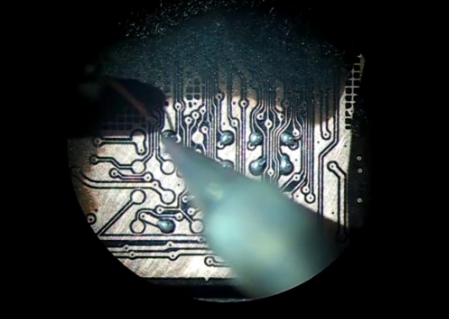
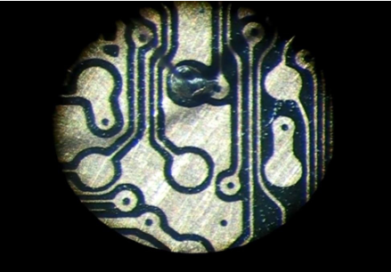
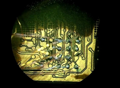 Once all contacts are soldered, ensure that none of the contacts are connected to the GND layer! All pins must be very tight!
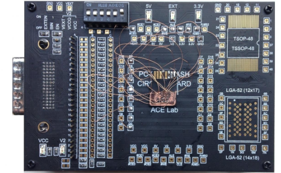 Now we are ready to connect our PCB to the PC-3000 FLASH and start the reading process!
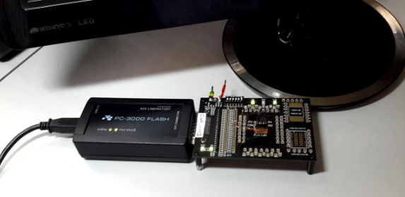 Source: How to Recover Data from Monolithic FLASH Chip Encapsulation (micro SD Card/TF Card) – Suzhou PanShou Data Recovery | Focused on SSD Data Recovery! http://www.4f61.com/article/707.html
Submission/Recruitment/Promotion/Advertising Please add WeChat:15989459034