How many steps are needed to put an elephant in the fridge? Three steps: open the fridge door, put in the elephant, and close the door. So how many steps are needed to create a chip? Also three: design the chip, manufacture the chip, and finally package and test the chip. However, is making a chip really that simple? Clearly not. Recently, an article titled “How Long Can 100 Million in Funding Last for a Chip Startup” went viral on many people’s social media feeds, which included the statement, “When the 100 million runs out, many companies haven’t even seen a glimpse of the chip; they may not even have a decent demo.”Yes, 100 million might buy a luxury apartment, but it may not be enough to support a chip from design to mass production. And this is only for chips using mature processes; for advanced process chips, the funding required is staggering, with the design cost for a 5nm chip reaching as high as $476 million.Today, I will explain how many steps are truly needed to create a chip from scratch and why it is so “money-consuming”?
Chip Design
Many people compare the process of manufacturing chips to building a skyscraper. So what is the first and most important step? Of course, it is the blueprint of the skyscraper, which is the chip design. In other words, chip design is the foundation of creating a chip; even if the downstream manufacturing and testing capabilities are exceptional, without a blueprint, it is useless.As one of the most intricate and grand projects in the world, chip design is not as simple as drawing pictures on a computer. Generally, the chip design phase can be divided into four major processes: specification definition, system-level design, front-end design, and back-end design.
1
Specification Definition
Specification definition is when engineers conduct a demand analysis at the beginning of chip design, determining the cost control level, purpose, and performance of the chip, completing the product specification definition to establish the overall direction of the design. They then check the agreements that need to be met; otherwise, the chip will not be compatible with products on the market and cannot connect with other devices. Finally, they establish the implementation methods of the chip, allocating different functions into different units and establishing connection methods between different units, thus completing the specification formulation. The purpose of chip specification definition is to ensure that the designed chip has no errors.
2
System-Level Design
Since chip design needs to comprehensively consider system interactions, functions, costs, power consumption, performance, security, and testability, engineers need to develop design solutions and specific implementation architecture designs based on the preliminary specification definitions, defining module functions and clarifying the chip architecture, business modules, power supply, etc., in the system-level design, such as CPU, GPU, NPU, RAM, connections, interfaces, etc.
3
Front-End Design
Front-end design of the chip, also known as logical design, can be said to be the soul of the entire chip design phase, truly realizing the process of creating a chip from nothing. Therefore, front-end design engineers have become the most sought-after talent in the industry, and their salaries naturally rise. However, what does front-end design mainly include?Front-end design is when engineers conduct specific circuit designs for each module based on the system design determined solutions, using Verilog or VHDL code (hardware description language) to describe the specific circuit implementation at the RTL (Register Transfer Level) level. In simple terms, it is to describe the module function in code, meaning the actual hardware circuit function is described using HDL language, forming RTL code. The code corresponds to the circuit, so when front-end design engineers write code, they need to know what kind of circuit the code will turn into.Once the code is generated, it needs to undergo simulation verification, strictly following the established specification standards, repeatedly testing the correctness of the code design through simulation verification. Verification is the most time-consuming and labor-intensive process in chip design. According to ARM technical white papers, 40% of a project’s resources are spent in the verification phase.After verification, logical synthesis is required, using EDA tools to convert the RTL description of the register transfer level design into a netlist to ensure that the circuit meets the standard in terms of area, timing, and other target parameters. Then, static timing analysis is performed, applying specific timing models to analyze whether the specific circuit violates the timing constraints set by the designer.The front-end design process is not a one-time effort; engineers need to repeatedly synthesize, verify, and conduct various design rule checks to ensure both the correctness of the design and that the layout and routing are feasible and optimized.
4
Back-End Design
Back-end design is the realization of front-end design; specifically, it involves converting the logical synthesis into a physical netlist and then converting it into graphic files that can be used by manufacturing plants to create photomasks.The first step is DFT (Design For Test), which is testability design. Chips often come with built-in testing circuits that need to be pre-planned and inserted into various logic circuits used for chip testing.Next is layout planning, which involves placing the macro unit modules of the chip, determining the placement of various functional circuits, such as IP modules, RAM, and I/O pins. The chip’s area, timing convergence, stability, and routing complexity are all influenced by the layout planning.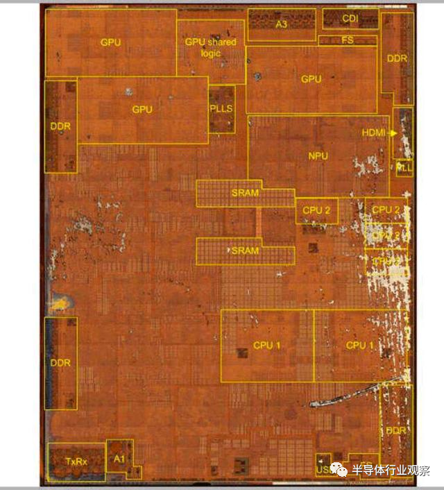 Apple A11 Layout PlanningThen, clock tree synthesis is carried out, which involves routing the clock and connecting various components. Since clock signals play a global coordinating role in digital chips, they are symmetrically connected to various register units, minimizing clock delay differences when the clock reaches each register from the same clock source, so separate routing is often required.After clock routing, normal signal routing is performed, including routing between various standard cells (basic logic gates); parasitic parameters are extracted, and signal integrity issues are re-analyzed and verified; finally, various verifications are conducted, and GDS layouts for chip production are generated.As the last step before chip production, back-end design often faces many challenges and tight deadlines. As we enter the nanometer era, with increasing layout and routing complexity, its importance is becoming more prominent. However, for some small and medium-sized design companies, having an excellent back-end design team and minimal capital expenditures is like trying to have both fish and bear’s paw; cultivating a complete back-end team is too costly and can exacerbate already tight finances. However, without back-end design, relying solely on front-end engineers may lead to significant redundancy in project experience, potentially affecting the chip’s final performance and power consumption. In this context, finding the best balance between the two, maximizing capital expenditure efficiency, becomes crucial, which cannot be achieved solely by the companies themselves but requires the support of professional teams.In fact, many chip companies choose to outsource back-end design to chip design service companies. Yes, this has led to another division of labor in the industry: chip design service companies, which neither belong to chip design enterprises nor wafer manufacturing enterprises, but are an inevitable result of the development of the chip industry, bridging the gap between chip design companies and wafer foundries. Well-known companies such as Creative Electronics, Chipown, Moore Elite, and Zhi Yuan Technology belong to chip design service enterprises.It can be said that chip design services play a role as a chip design foundry center in the chip industry chain, providing immense value to chip design companies, especially startup design firms. Their comprehensive back-end design services are one of the most important values. Generally, chip design service companies have rich experience in back-end design; for example, Creative Electronics, as a full-process customized IC design service company, is also very professional in digital back-end (DFT, STA, APR) and can provide comprehensive DFT services. Moore Elite is a leading one-stop chip design and supply chain service platform in China, committed to ensuring “there are no difficult chips to make in China”; in the field of chip design services, Moore Elite offers ASIC design and turnkey solutions, with a stable back-end design team that has extensive experience in SoC design and project management, providing digital back-end design aimed at advanced process nodes. Although Canxin Semiconductor’s business mainly includes IP and chip customization services, its chip customization services cover both front-end and back-end, and its strength cannot be underestimated.As Moore’s Law continues to evolve, along with the trends of miniaturization and integration, back-end design is becoming increasingly complex and important. Unlike those financially robust system vendors and internet companies, startup chip companies must understand how to “travel light” and quickly bring chips to market with the lowest risk and cost possible.
Chip Manufacturing
Chip manufacturing is a crucial step in turning chips from blueprints into physical objects, but before mass production, there is another important step called wafer processing, commonly referred to as trial production.For chip developers, wafer processing is akin to a test for students; students “turn pale at the thought of exams,” while chip developers “turn pale at the thought of wafer processing.” The reason is that the cost of a failed wafer processing can be severe; a single failure often means losses of hundreds of thousands or even millions and a missed market opportunity of at least six months. Many startup chip companies have disappeared in the vast sea of the chip industry due to failed wafer processing. The reasons for wafer processing failures are varied; it could be as simple as reversing VDD and GND or using the wrong liquid for wet cleaning; in short, any small oversight could lead to a failed wafer processing.Returning to the main topic, how many steps are involved in chip manufacturing, and why can it make companies “turn pale at the thought of wafer processing”? It is understood that a chip production line involves approximately 2000-5000 processes. I may not be able to cover all the details, so I will only introduce some key steps.From a broad perspective, wafer production includes two major steps: crystal rod manufacturing and chip manufacturing, along with wafer probing processes, collectively referred to as the front-end wafer manufacturing processes, while the packaging and testing mentioned below are referred to as the back-end wafer manufacturing processes.
1. Purification: Sand/quartz is purified to obtain silicon dioxide with a silicon content of 25%, then refined using an electric arc furnace, chlorinated with hydrochloric acid, and distilled to obtain high-purity crystalline silicon with a purity of over 99%.
2. Crystal Rod Manufacturing: Crystalline silicon is melted at high temperatures and pulled using a rotational stretching method, growing through neck growth, crystal crown growth, crystal growth, and tail growth to obtain a complete crystal rod.
3. Slicing: The crystal rod is sliced horizontally using a ring saw with diamond particles embedded in its inner diameter edge, cutting it into wafers of consistent thickness.
4. Polishing: The wafer’s appearance is polished to remove saw marks and damage caused during cutting, ensuring the wafer surface meets the required smoothness.
5. Oxidation: The surface undergoes oxidation and chemical vapor deposition, serving as an auxiliary layer for later processes and assisting in isolating electrical devices to prevent short circuits.
6. Photolithography and Etching: A layer of photoresist is spun on the oxidized wafer surface, exposed, and then developed to reveal the circuit pattern. Chemical reactions or plasma bombardment are then used to transfer the circuit pattern onto the wafer surface.
7. Ion Implantation and Annealing: Impurity ions are bombarded into the semiconductor lattice, and the ion-implanted semiconductor is heated at a certain temperature to activate different electrical properties of the semiconductor material.
8. Vapor Deposition and Plating: Vapor deposition is used to form various metal layers and insulating layers, while plating is specifically for growing copper interconnect metal layers.
9. Chemical Mechanical Polishing: A combination of chemical etching and mechanical polishing is used for polishing.
10. Finally, multiple layers of circuits and components are processed and manufactured on the wafer.
11. Wafer Probing Process: Each die is tested for its electrical characteristics using a probe tester, discarding any non-compliant dies.
Chip Packaging and Testing
Packaging and testing refer to the back-end processes of wafer manufacturing mentioned earlier. Packaging is the process of processing the tested wafers into chips, while testing involves checking defective chips, including wafer testing before packaging and finished product testing.As the last mile before chip production, packaging and testing are also crucial steps for the finished chip. Packaging protects, supports, connects, dissipates heat, and ensures reliability for the chip, while testing ensures chip quality and even enhances shipping quality, preventing defective chips from being released. Specifically, the packaging and testing steps can be divided into:
1. Backside Thinning: The wafer is thinned from the backside to reach the required thickness for packaging.
2. Wafer Dicing: The wafer is diced into individual dies, which are then cleaned.
3. Optical Inspection: Checking for any defects.
4. Chip Bonding: Chips are bonded, silver paste is cured (to prevent oxidation), and leads are soldered.
5. Injection Molding: To prevent external impacts, the product is encapsulated using EMC (encapsulating material) while being heated to harden.
6. Laser Marking: The production date, batch number, and other information are engraved on the product.
7. High-Temperature Curing: Protecting the internal structure of the IC and eliminating internal stress.
8. Excess Material Removal: Trimming edges.
9. Plating: Enhancing conductivity and improving solderability.
10. Forming and inspecting for defects.
11. Chip Testing: This includes general testing and special testing; general testing assesses the electrical characteristics of the chip, categorizing them into different grades based on these characteristics. Special testing is targeted and specific, checking if the chip meets customer-specific requirements.
12. Qualified products are labeled with specifications, models, and manufacturing dates before being packaged for shipment.
Final Thoughts
Chip manufacturing is indeed a money-burning industry. To truly achieve mass production of a chip, each of the aforementioned steps is critical. For startup companies lacking in personnel, funds, and resources, even the four major processes in the chip design phase are difficult to cultivate a professional team. As mentioned in the article “How Long Can 100 Million in Funding Last for a Chip Startup,” many founders spend their days in meetings, managing, and raising funds, while at night returning to the company to work on technology.No startup’s success is smooth sailing; the pressures they face are unimaginable to ordinary people, and the situation is constantly changing. Setbacks are inevitable, but how to navigate towards success with minimal detours is controllable. The key is to find the most suitable solutions for themselves, which is the direction many chip startups are striving for.
Disclaimer: This article is purely for practical discussion purposes, and the copyright belongs to the original author and related rights holders. The views represent the author’s personal opinions. If there are any issues, please contact us, and we will handle them promptly.