How Image Sensors Drive the Development of Embedded Vision Technology

How Image Sensors Drive the Development of Embedded Vision Technology

New imaging applications are booming, from collaborative robots in Industry 4.0 to drone firefighting or agriculture, to biometric facial recognition, and handheld medical devices in homes. A key factor in the emergence of these new application scenarios is that embedded vision is more prevalent than ever. Embedded vision is not a new concept; it simply defines a system that includes a vision setup that controls and processes data without an external computer. It has been widely used in industrial quality control, with the most familiar example being the “smart camera.”

In recent years, the development of cost-effective hardware components in the consumer market has significantly reduced the bill of materials (BOM) costs and product size compared to previous computer-based solutions. For example, small system integrators (OEMs) can now procure single-board computers or module systems like NVIDIA Jetson in small quantities; larger OEMs can directly obtain image signal processors like Qualcomm Snapdragon. On the software level, available software libraries can accelerate the development speed of dedicated vision systems and reduce configuration difficulties, even for small batch production.

The second change driving the development of embedded vision systems is the emergence of machine learning, which allows neural networks in laboratories to be trained and then directly uploaded to processors so that they can automatically recognize features and make decisions in real-time.

Providing solutions suitable for embedded vision systems is crucial for imaging companies targeting these high-growth applications. Image sensors play an important role in large-scale adoption as they can directly influence the performance and design of embedded vision systems, with their main driving factors summarized as: smaller size, weight, power, and cost, abbreviated in English as “SWaP-C” (decreasing Size, Weight, Power, and Cost).

1

Reducing Costs is Crucial

The accelerator for new applications in embedded vision is the price that meets market demand, and the cost of vision systems is a major constraint to achieving this requirement.

1

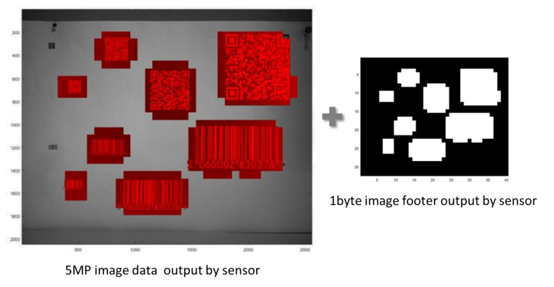
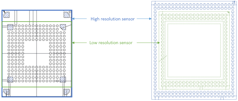
Saving Optical Costs

The first way to reduce the cost of vision modules is to minimize product size, for two reasons: first, as the pixel size of the image sensor decreases, more chips can be manufactured from the wafer; on the other hand, sensors can use smaller, lower-cost optical components, both of which can reduce inherent costs. For example, Teledyne e2v’s Emerald 5M sensor reduces pixel size to 2.8µm, allowing M12 lenses to be used on five-million-pixel global shutter sensors, resulting in direct cost savings—the entry-level M12 lens costs about $10, while larger C or F mount lenses cost 10 to 20 times more. Thus, reducing size is an effective way to lower the cost of embedded vision systems.
For image sensor manufacturers, this reduced optical cost has another impact on design because, generally speaking, the lower the optical cost, the less ideal the sensor’s incident angle. Therefore, low-cost optics require specific displacement microlenses to be designed above the pixels so that they can compensate for distortion and focus light from wide angles.

2

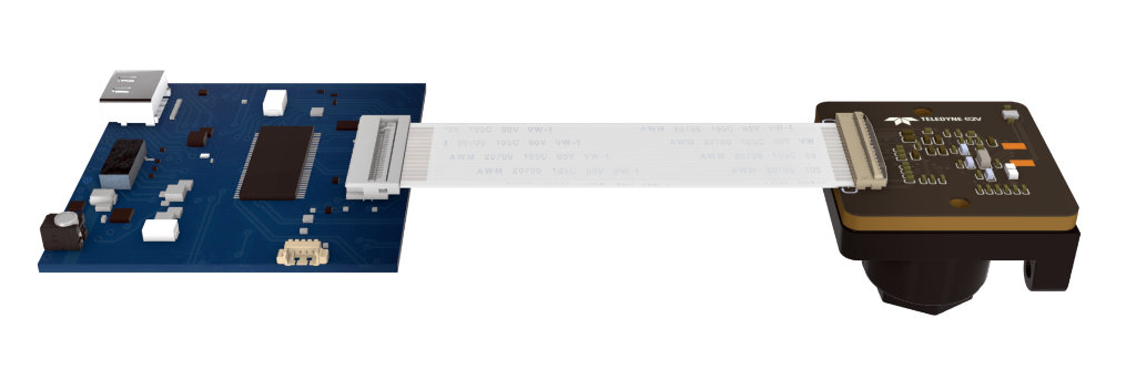
Cost-Effective Sensor Interfaces

In addition to optical optimization, the choice of sensor interface also indirectly affects the cost of vision systems. The MIPI CSI-2 interface is the most suitable choice for achieving cost savings (it was originally developed by the MIPI Alliance for the mobile industry). It has been widely adopted by most ISPs and has begun to be used in the industrial market because it provides a lightweight integration from low-cost System on Chip (SoC) or System on Module (SoM) from companies like NXP, NVIDIA, Qualcomm, Rockchip, Intel, and others. Designing a CMOS image sensor with a MIPI CSI-2 sensor interface allows data from the image sensor to be transmitted directly to the host SoC or SoM of the embedded system without any bridging, saving costs and PCB space; of course, this advantage is even more prominent in multi-sensor-based embedded systems (such as 360-degree panoramic systems).
However, these benefits are subject to some limitations. The widely used MIPI CSI-2 D-PHY standard in the machine vision industry relies on cost-effective flat ribbon cables, which have the drawback of limiting connection distances to 20 centimeters, which may not be ideal for remote gimbal setups where the sensor is far from the main processor, as is often the case in traffic monitoring or surround view applications. One solution to extend the connection distance is to place additional repeater boards between the MIPI sensor board and the host processor, but this sacrifices miniaturization. There are other solutions not from the mobile industry but from the automotive industry: the so-called FPD-Link III and MIPI CSI-2 A-PHY standards support coaxial or differential pairs, allowing connection distances of up to 15 meters.

3

Reducing Development Costs

When investing in new products, the continually rising development costs often pose a challenge, potentially costing millions in non-recurring engineering (NRE) and putting pressure on time to market. For embedded vision, this pressure becomes greater because modularity (i.e., whether the product can switch between multiple image sensors) is an important consideration for integrators. Fortunately, one-time development costs can be controlled by providing a certain degree of cross-compatibility between sensors, such as by defining combined/shared identical pixel structures for stable photoelectric performance, sharing a single front-end structure through the same optical center, and compatible PCB components (by size compatibility or pin compatibility), thereby accelerating evaluation, integration, and the supply chain, as shown in Figure 1.
How Image Sensors Drive the Development of Embedded Vision Technology
Figure 1: Image sensor platforms can provide pin compatibility (left) or size compatibility (right) for proprietary PCB layout design.
Today, with the widespread release of so-called module and board-level solutions, the development speed of embedded vision systems is faster and more affordable. These one-stop products typically include a sensor board that can be integrated at any time, sometimes including a preprocessing chip, a mechanical front, and/or a lens interface. These solutions benefit applications by highly optimized sizes and standardized connectors, allowing them to connect directly to off-the-shelf processing boards like NVIDIA Jetson or NXP i.MX ones without the need to design or manufacture intermediate adapter boards. By eliminating the need for PCB design and manufacturing, these module or board-level solutions not only simplify and accelerate hardware development but also significantly shorten software development time, as they are mostly provided with Video4Linux drivers.
Therefore, original equipment manufacturers and vision system manufacturers can skip weeks of development time in making the image sensor communicate with the main processor, allowing them to focus on their unique software and overall system design. Optical modules, such as those provided by Teledyne e2v, offer a complete package from optics to drivers to sensor boards by integrating the lens within the module, eliminating tasks related to lens assembly and testing, further driving the development of one-stop solutions.
How Image Sensors Drive the Development of Embedded Vision Technology
Figure 2: New modules (right) allow direct connection to off-the-shelf processing boards (left) without the need to design any additional adapter boards.

2

Improving Autonomous Energy Efficiency

Due to external computers hindering portable applications, battery-powered devices are the most obvious application benefiting from embedded vision. To reduce system energy consumption, image sensors now incorporate multiple functions that enable system designers to save energy.
From the perspective of the sensor, there are various ways to reduce the power consumption of vision systems without compromising the acquisition frame rate. The simplest method is to minimize the dynamic operation of the sensor itself at the system level by using standby or idle modes for as long as possible, thereby reducing the power consumption of the sensor itself. Standby mode reduces the sensor’s power consumption to less than 10% of its working mode by turning off the emulation circuits. The idle mode can halve the power consumption and allows the sensor to restart and capture images in microseconds.
Another energy-saving method is to adopt more advanced lithography node technologies to design sensors. The smaller the technology node, the lower the voltage required to switch transistors, which reduces dynamic power consumption because power consumption is proportional to the square of the voltage. Therefore, pixels produced using 180nm technology ten years ago not only reduced the transistors to 110nm but also lowered the voltage of the digital circuits from 1.8V to 1.2V. The next generation of sensors will use a 65nm technology node, making embedded vision applications more energy-efficient.
Lastly, by selecting the appropriate image sensor, it is possible to reduce the energy consumption of LED lights under certain conditions. Some systems must use active illumination, such as generating three-dimensional maps, motion freezes, or simply using sequential pulses at specified wavelengths to enhance contrast. In these cases, reducing the noise of the image sensor in low-light environments can achieve lower power consumption. By decreasing sensor noise, engineers can determine whether to reduce current intensity or the number of LED lights integrated into the embedded vision system. In other cases, when image capture and LED flashing are triggered by external events, choosing the appropriate sensor readout structure can significantly save energy. When using traditional rolling shutter sensors, LED lights must be fully on during full-frame exposure, while global shutter sensors allow only parts of the frame to activate the LED lights. Therefore, using a global shutter sensor instead of a rolling shutter sensor when employing pixel-level correlated double sampling (CDS) can save illumination costs while maintaining low noise similar to CCD sensors used in microscopes.

3

On-Chip Functions Pave the Way for Vision System Programming

Some extended concepts of embedded vision guide us to comprehensively customize image sensors by integrating all processing functions (system on chip) in a 3D stacked manner to optimize performance and power consumption. However, the cost of developing such products is very high; achieving this level of integration with fully customized sensors is not entirely impossible in the long run, but we are currently in a transitional phase that includes embedding certain functions directly into the sensor to reduce computational load and speed up processing time.
For example, in barcode reading applications, Teledyne e2v has patented technology that incorporates an embedded function with a proprietary barcode recognition algorithm into the sensor chip, which can identify the location of barcodes within each frame, allowing the image signal processor to focus only on these areas, improving data processing efficiency.
How Image Sensors Drive the Development of Embedded Vision Technology
Figure 3. Teledyne e2v Snappy five-million-pixel chip automatically identifies the location of barcodes.
Another function that reduces processing load and optimizes

Leave a Comment