
Today, let’s talk about how chips are born from the manufacturing perspective.
From a handful of sand that can be easily tossed, to the chips that are indispensable in various industries, it goes through hundreds or even thousands of processing steps. The first step is to transform sand into monocrystalline silicon.

The main component of sand is silicon dioxide, which contains the silicon element needed for chips.
However, to truly manufacture chips, the purity of the silicon raw material is extremely high — at most, there can only be one impurity atom among 100 million silicon atoms.
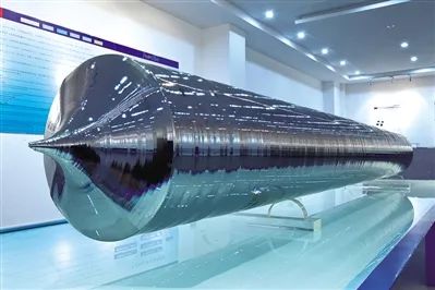
Therefore, sand needs to be repeatedly purified, and then shaped or pulled in a furnace at high temperatures through zone melting or the Czochralski process to obtain silicon monocrystalline rods (monocrystalline silicon rods) with a purity requirement of 99.9999%.
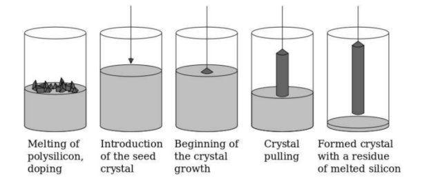
After obtaining the monocrystalline silicon rod, horizontal cutting can yield many cylindrical monocrystalline silicon wafers. This silicon wafer is what we commonly refer to as a wafer.
The larger the diameter of the wafer, the more difficult it is to manufacture, and the more chips can be cut from it. Currently, the mainstream wafer diameter is 12 inches (approximately 30cm).
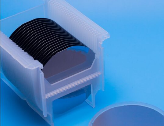
After slicing, the wafers also need to go through grinding, polishing, and cleaning processes to ensure that the surface of the wafer is cleaner and smoother than a mirror, facilitating the subsequent circuit etching.
At this stage, we’ve only laid the “foundation” for building the chip; we are still far from the chip itself, as the next steps involve the most advanced technology.
An integrated circuit, as the name suggests, integrates the designed circuit in a stacked form, much like building a city.
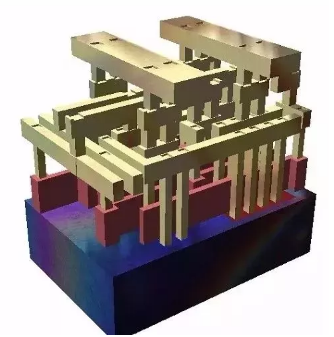
This is why it is often said in the industry that making chips is like building houses.
How to implement the designed circuit layout on the wafer? This involves many steps.
1. Photolithography
Photolithography is a very important process in chip manufacturing and is the core process that determines the integration level of the chip.
Before photolithography, a liquid photoresist needs to be coated on the wafer, a step also known as spin coating. This allows the photoresist to become thin and uniform.
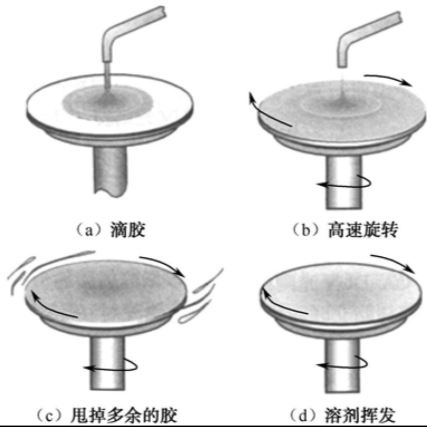
The photoresist layer is exposed to ultraviolet light through a mask, becoming soluble; the mask prints the pre-designed circuit pattern, and the ultraviolet light passing through it illuminates the photoresist layer, forming the circuit patterns for each layer. This principle is similar to old film exposure.
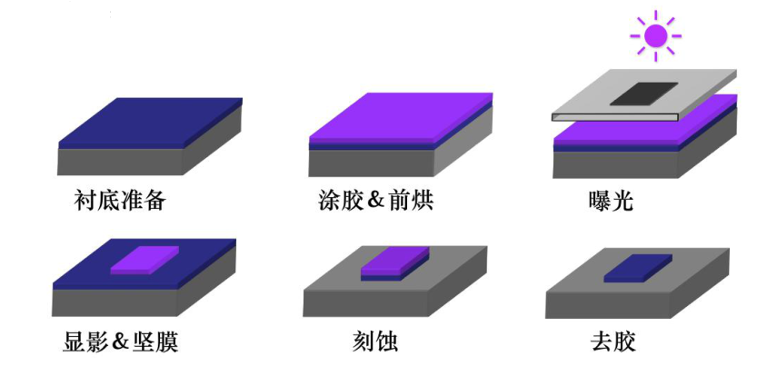
In other words, through a series of steps such as spin coating, pre-baking, exposure, development, and hardening, specific parts of the thin film on the wafer surface are removed, leaving a thin film with micro-pattern structures. This allows the designed circuit patterns to be transferred from the photomask to the photoresist on the wafer surface.
This requires photolithography equipment to have very high pattern resolution and sensitivity, and to ensure low defect levels.
Generally, throughout the semiconductor device manufacturing process, many photolithography steps are performed, and more complex integrated circuits may require up to 50 photolithography steps.
2. Etching
Etching is closely related to photolithography.
Etching involves removing the parts of the wafer that are not covered by the photoresist through chemical reactions or physical actions, leaving behind the required circuit structure.
Etching technology is mainly divided into dry etching and wet etching. Dry etching mainly uses reactive gases and plasma for etching; wet etching mainly uses chemical reagents to chemically react with the material being etched.
3. Doping
Diffusion and ion implantation are the main doping processes.
This step involves controllably introducing the required impurities into specific areas of the wafer, altering the electrical properties of the semiconductor to enhance conductivity, ultimately forming N or P regions.
After etching and ion implantation are completed, the mission of the photoresist is finished; once the photoresist is removed, the designed circuit patterns can be obtained. By this point, the transistors are essentially complete.
Next, additional steps such as polishing, forming electrodes, and wafer testing will be performed. Afterward, the wafer will be cut into individual dies.
The chips we commonly see are actually the products obtained after packaging.
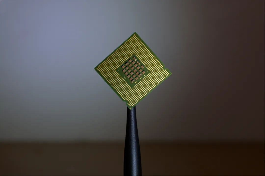
Packaging involves interconnecting the chip’s solder pads with the external pins of the package, and then encasing the chip with insulating materials.
This not only protects the chip from damage, ensuring its performance and facilitating transport, but it also connects the chip components/circuit modules together through interconnections.
Next is the chip testing phase, which usually includes aging tests, finished product inspections, and reliability tests. Through testing, defective products are eliminated, leaving behind flawless chip products.
Thus, the chips essential for our daily lives are born.
Note: Some images and content reference the internet.
Reproduced content only represents the author’s views